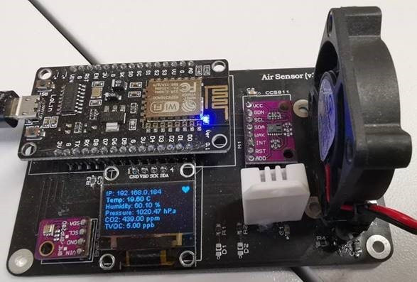
Some time ago I had reason to log the quality of air in a room. We needed to know what the levels of carbon monoxide and carbon dioxide were at a given time. I quickly produced a thing on a strip of veroboard that would use an ESP8266 to log over WiFi to the ThingSpeak platform. This proved to be useful, and so I made a couple more on a PCB for various other locations.
The sensor uses a CCS811 (a low-power digital gas sensor) , BME280 (sensor measuring relative humidity, barometric pressure and ambient temperature) and DHT22 (capacitive humidity sensing digital temperature and humidity) sensors, with an OLED display and a small 5V 40mm fan to waft some air around prior to taking a reading. In reality the project no longer needs the DHT22 sensor, since the BME280 device provides better temperature and humidity measurements and adds air pressure readings. But it is included for historical reasons on my project. Feel free to omit it!
The project is very simple, as it just hooks up modules purchased from eBay. The modules cost less than £2 each at the time of writing and came from eBay or AliExpress.
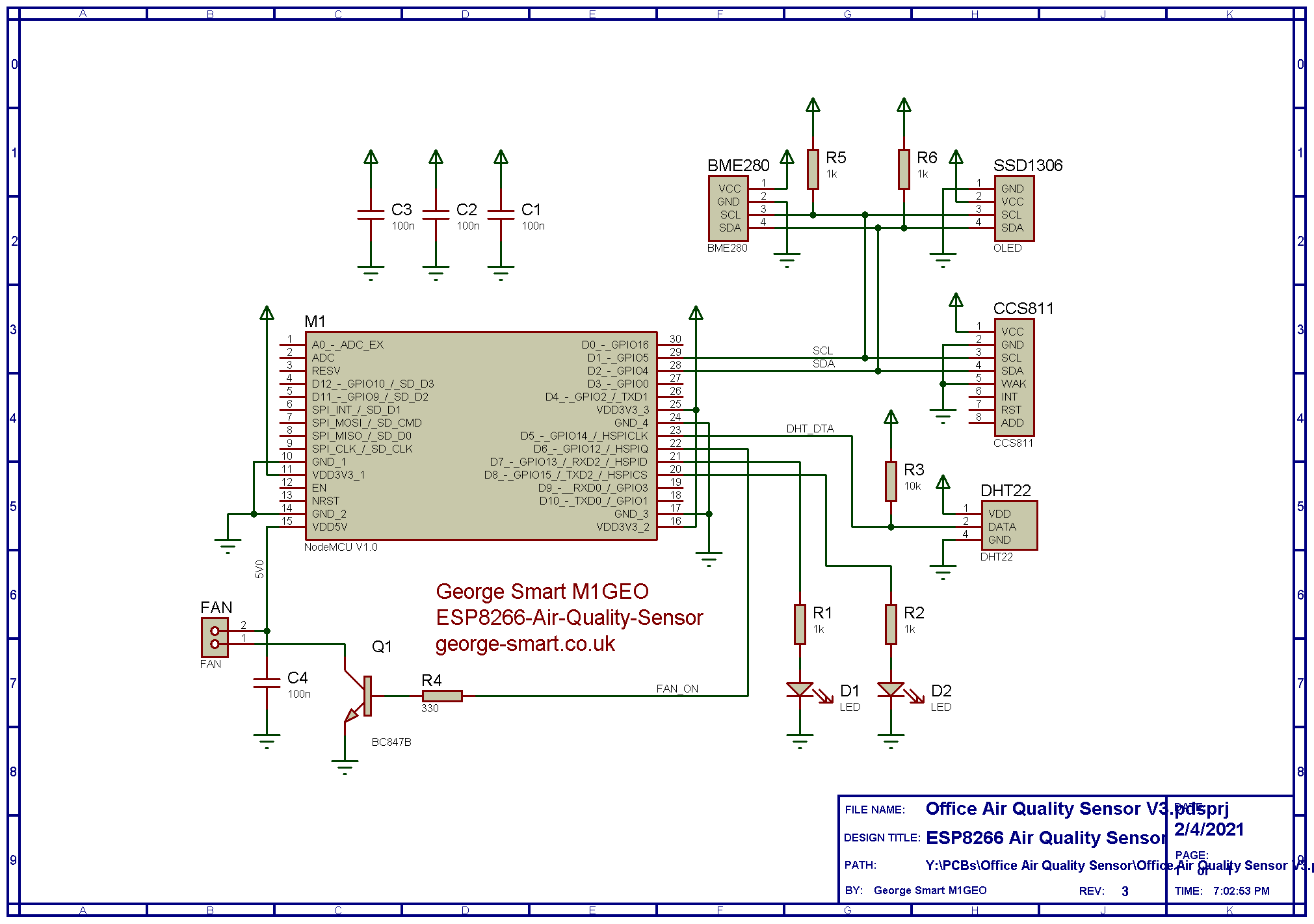
Since this time, others have asked me for the design files, and so I have now shared them on GitHub: github.com/m1geo/ESP8266-Air-Quality-Sensor. The link contains everything you need to create your own! PCB files, source code and schematic.
If you follow the GitHub link above, you fill find two folders. These are explained in the subsequent sections below.
Code
The code folder contains the Arduino code which runs on the ESP8266 device. You’ll need to source libraries for the SSD1306 OLED, the DHT22 (or cheaper DHT11), the Adafruit BME280 module, and the Adafruit CCS811 module. All these are available inside the Arduino IDE.
The MCU board used is a ESP8266 NodeMCU 1.0. This, and all the modules are easily sourced from the usual places (eBay, AliExpress, etc.), and are cheap. You’ll need to create a ThingSpeak account and then enter your API Key and channel number into the source code, as well as your WiFi name and passcode.
Board
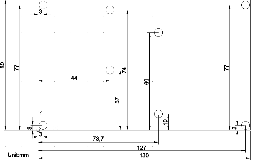
The board folder contains an example schematic design and basic PCB gerber files. You can use these gerber files to have a PCB made. All the cheap PCB houses will produce this board fine. The board files supplied are for the board shown above.
As I was unable to take part in the CQWW CW Contest 2020 due to Coronavirus COVID-19 regulations, I decided to experiment with using the wideband SDR of the Hermes Lite 2 SDR (HL2).
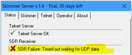
The process appeared to be quite smooth, however upon completion, the CW Skimmer’s Skim Server (SkimSrv) would report that the SDR connection had timed out. This transpired to be the hardware watch dog timer (WDT) timeout inside the FPGA on the Hermes Lite 2 – a precaution to stop the SDR from being stuck in transmit should the connection to it drop:
The solution was two-fold:
Update the HL2 gateware to a version allowing the WDT to be adjusted/disabled
Update the SkimSrv DLL plugin to a version using the WDT configuration
Getting the Latest HL2 Gateware
The gateware of the HL2 is a bit like what you may consider as firmware. Only, firmware is code that runs on a CPU or microcontroller, and gateware is code that configures the internal connections of an FPGA. This difference is immaterial here, but it is useful to know.
There are many versions of gateware available for the Hermes Lite 2. You are best advised to hunt around Steve Haynal KF7O’s project repositories for the Hermes-Lite2 under the gateware\bitfiles folder and find a version that best suits your needs. It is important to note that some of the gateware files in these folders are compiled with special features and are often not recommended for general use. Here I will cover two versions that I find interesting. The first is the standard gateware that supports both transmit and receive on 4 slices. The second receive only gateware swaps the transmit logic for extra receive logic, resulting in 10 receive-only slices.
One final note, the links I provide are for Hermes-Lite 2.0 build5 and later. If you have an earlier build, then there are different files required which are also present in the variants folders.
Standard 4-slice TX/RX gateware
I started off by finding the latest “testing” version of the HL2 gateware, which can be found in the repositories mentioned above. At the time of writing the original article “testing/20201107_72p5” was the latest version that was recommended for more general use. Since the original publication of this post, this has been rolled into the stable/20201212_72p8 release.
Once you have read the readme and are happy with the notes supplied with the version of the bitfile (the actual compiled file the FPGA is sent to configure itself), then you are ready to go.
Use stable/20201212_72p8/hl2b5up_main/hl2b5up_main.rbf (direct link to download) which supports up to 4 receiver slices, but also includes transmit and is suitable for general use – again – read the notes that are supplied! They are important. Whatever you chose, you may need to rename the “.rbf” file to “hl2b5up_main.rbf” to allow it to be flashed by SparkSDR. Quisk doesn’t seem to care what the file is called.
No transmit 10-slice receive gateware
My actual reason for changing the gateware was to try the 10-slice receive gateware for use with SparkSDR as a grabber for CW Skimmer, as well as all of the other digital modes (RTTY, PSK, WSPR, FT8, JT65, etc.).
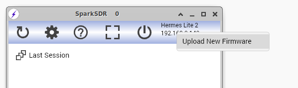
To program the gateware there are two options. I opted to use SparkSDR2 by Alan Hopper M0NNB. The process is easy and SparkSDR2 supports Windows and Linux. Run SparkSDR, press the discovery button (the rotating arrow on the left) until your Hermes Lite 2 is discovered, and then right-click and select firmware. From there, navigate from the downloaded and renamed file “hl2b5up_main.rbf” and press program. It should take around a minute.
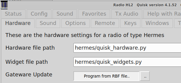
You are also able to use Quisk by James Ahlstrom N2ADR. From the Config dialogue, select your radio, and then select “Program from RBF file”. The update should not take long.
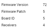
Once the upload is complete, you should power cycle the Hermes Lite 2 SDR, and then check in your favourite program that the update was successful. I checked that the radio still worked, and I could see that the revision gateware had changed to what I expected within SparkSDR: “Version 72 Patch 5” (now superseded by stable 72p8) and that I did indeed have 4 receivers available. If you used a different gateware version, you should see different results here:
Installing the recompiled HermesIntf.dll
Originally, the HermesIntf.dll file was provided by Vasiliy Gokoyev K3IT on the GitHub page HermesIntf. However, this DLL does not take advantage of the extra WDT options available in the HL2 gateware we just updated. To make such updates, this required the original DLL supplied by Vasiliy K3IT to be recompiled, incorporating changes from Steve KF7O’s gateware.
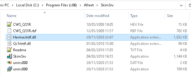
I was beaten to doing this by Robin Davies G7VKQ, who kindly shared the rebuilt DLL file with me on Twitter (thanks!!). This DLL file can be downloaded here: HermesIntf_G7VKQ.zip. There’s also a version by KV4TT (released Jan 2021) which I would suggest using as it has some further tweaks for handling the watchdog timer. This file is then to be copied into the SkimSrv folder, typically located within “C:\Program Files (x86)\Afreet\SkimSrv\” on a modern 64-bit version of Windows. You will of course need to install SkimSrv by Afreet Software from here. A trial version is available – you’ll need the Skim Server, not the standard CW Skimmer.
Once you’ve copied the DLL into the installation folder, you are ready to fire-up the SkimSrv. SkimSrv has a little icon in the system tray, as shown below. Click on this to open the SkimSrv settings dialogue.
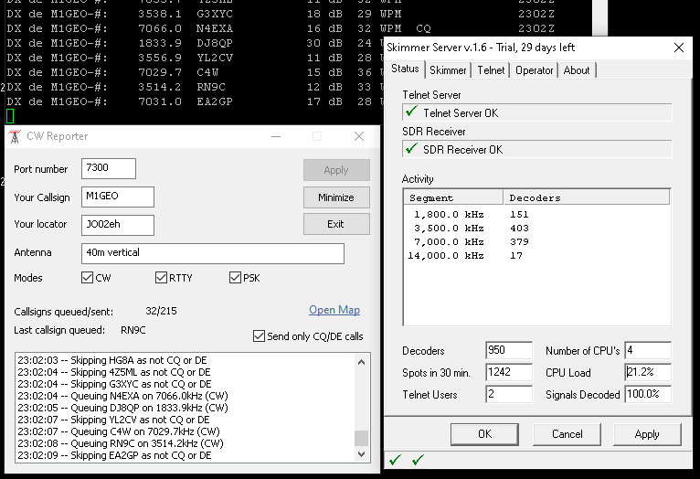
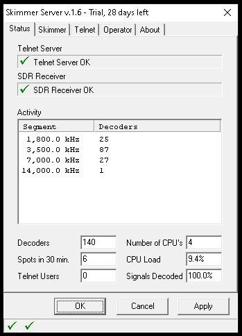
From here, you can use the Skimmer tab to set up the frequencies, sample rates, radios, etc., to use. This is all as you would expect and is pretty straight forward. Above, you can see I am using the 4 receivers available in the gateware version of the HL2 I chose. The image at the top of the page shows operation during CQWW CW 2020, where there were huge numbers of signals present on the bands.
You can connect a telnet program to “localhost” on port “7300” to connect to the Skimmer Server by default. This acts like a DX Cluster with spotting information.
Uploading to PSKReporter
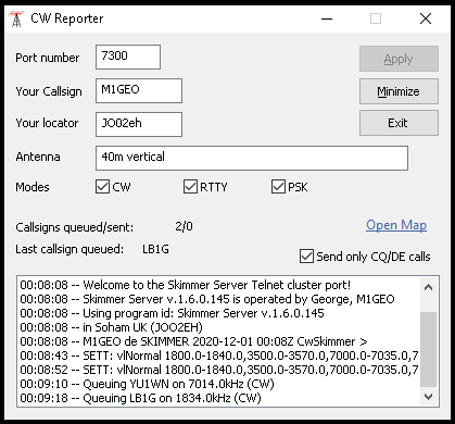
One of the most easy way is use CW Reporter by Philip Gladstone N1DQ. Philip runs PSKReporter, and, offers the CW Reporter application to interface between CW Skimmer Server and PSKReporter. It is easy to set up, working almost out of the box, and translates the DX Cluster style Telnet spots into reports for PSKReporter.info.
One comment to note here is that you should have calibrated your receiver’s frequency before doing this – otherwise, you may be spreading incorrect frequency information.
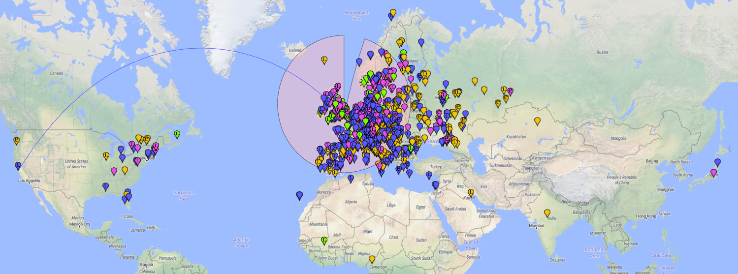
Finally, it is possible to see, on a map, using appropriate filters, what stations I have heard on CW over the past 24 hours:
Click any image to enlarge.
Thanks to everyone who offered help and suggestions along the way!
A key part of a GPS disciplined oscillator is the oscillator itself. During earlier testing I had used two Trimble 34310-T2 OCXO units and one seemed to perform much better than the other. I later read that this may be due to their aging, and that they gradually drift away from their optimal frequency – in this case, 10.000000 MHz – which in turn makes the phase-locked loop (PLL) struggle to converge the frequencies (and thus phase) of the loop. I also have a couple of IsoTemp 143-141 OCXOs, which I will measure, too.
The PLL compares the incoming phase of a reference frequency (here, derived from GPS timings) and the oscillator we’re ‘disciplining’. The loop can work in many ways, but, a common technique is to use digital signals from a phase-frequency detector though an analogue loop filter to generate some kind of voltage control voltage. This voltage is then fed back to the control pin of the oscillator, and the frequency changes accordingly. My post on using a Lattice FPGA development board to create a phase-frequency detector can be found in my Experiments with Phase-Frequency Detectors post.
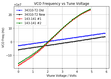
My first task was to characterise the relationship between frequency and control voltage. For this task, I used a networked spectrum analyser in frequency counter mode and power supply, writing a simple Python3 script to twiddle the control voltage and record the corresponding frequency. I settled on taking an average of 5 readings at each voltage, with the control voltage swept at 100mV intervals through the specified VCO range. I repeated this for each of the oscillators I was hoping to use.
The IsoTemp 143-141 units have a much wider tuning range when compared to the Trimble 34310-T2 modules. In practice this means that the Trimble devices will have greater frequency resolution since they cover a smaller tuning range for the same control voltage range.
Another practical aside is that the IsoTemp 143-141 is a single-ovened oscillator whereas the Trimble 34310-T2 is a double-ovened module. This means that the Trimble unit is much less prone to external thermal variation. However, the IsoTemp unit as a larger tuning range, which will help the PLL keep in lock when there are large temperature variations.
The nominal 10 MHz frequency is found at the following tune voltage for each unit:
OCXO Unit
Approx. Tuning Voltage (V)
Measured Frequency (Hz)
34310-T2 Old
1.90
10000000.03
34310-T2 New
3.70
10000000.04
143-141 #1
2.10
10000000.18
143-141 #2
2.00
9999999.78
It is clear from this that “34310-T2 New” is skewed to a higher voltage than the older Trimble unit.
I also observed the warmup time for each of the oscillator modules and the frequency of oscillation without any control voltage applied. Each unit was correctly orientated, supplied with the correct supply voltage as per the datasheet , and without any extra thermal insulation. The room temperature was 21C.
OCXO Unit
Approximate Oven Warmup Time (m)
Power Requirements (W)
Natural Frequency (Hz)
34310-T2 Old
~4 (sharp cut off)
Max: 8.60 Norm: 2.08
10000000.88 (ΔF: 0.88 Hz)
34310-T2 New
~4 (sharp cut off)
Max: 8.62 Norm: 2.00
9999996.80 (ΔF: -3.20 Hz)
143-141 #1
~5 (more gradual)
Max: 2.63 Norm: 1.03
9999999.01 (ΔF: -0.99 Hz)
143-141 #2
~5(more gradual)
Max: 2.61 Norm: 1.10
9999999.87 (ΔF: -0.13 Hz)
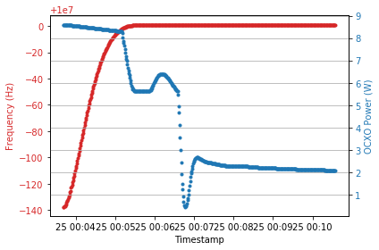
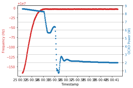
An example of the data captured during the warmup is given below for the Trimble units below:
34310-T2 Old:
34310-T2 New
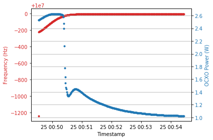
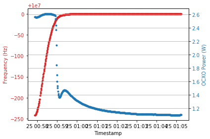
It is clear to see both Trimble units behave similarly, taking a similar time to warm up at around 4 minutes. The same data was obtained for both IsoTemp modules:
143-141 #1 – I suspect the first point at -1250 Hz is caused by measurement error and can be disregarded. This brings the unit inline with how #2 (below) responds
143-141 #2
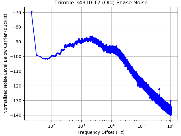
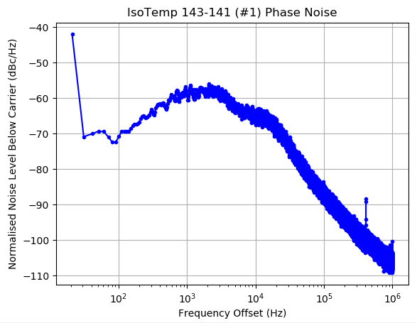
The next thing I would like to measure is the phase noise of both of the oscillator units. I have been playing around with scripting the measurement of phase noise of a signal using a spectrum analyser in clever ways. I am able to produce the following graphs. It is important to note that these graphs are not accurate!
A snippet from the IsoTemp 143 datasheet shows these measurements to be considerably distant from the expected results – again confirmation that the above graphs are not accurate.
For now, these are the best I am capable of producing. The numerical values are not absolute, although they should be comparable to those measured on a real noise analyser. However, they’re valid for an optician style “better-or-worse” comparison. I think it is fair to draw the conclusion that the phase noise of the Trimble unit is “better” than that of the IsoTemp unit. It is also worth noting that the output from the IsoTemp unit measured +13.5dBm (square wave), whereas the Trimble unit output only +5.3dBm (sine wave). This extra power required a slightly higher minimum attenuation in order to keep the spectrum analyser happy.
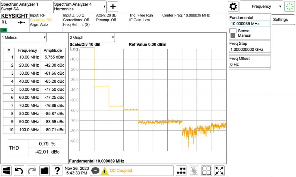
I also took the opportunity to look at the harmonic content for both types of oscillator. First the Trimble unit:
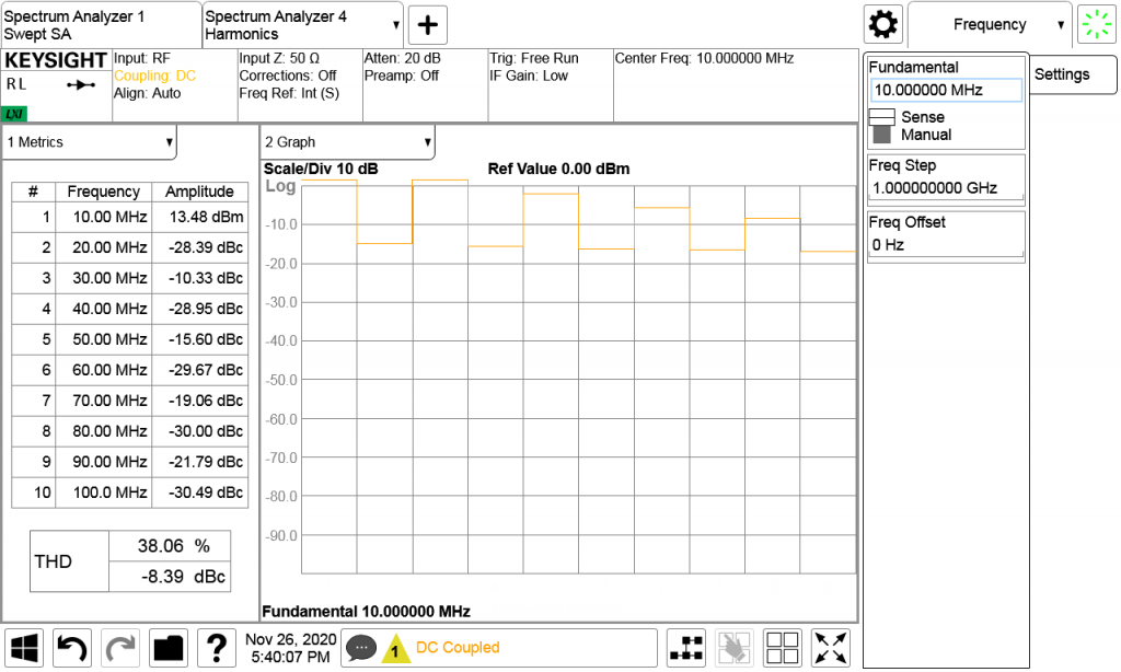
As expected, the IsoTemp produced high levels of odd-harmonics, which is to be expected given the square-wave output:
It seems that both the Trimble and IsoTemp parts are viable in the circuit I have been thinking of. The Trimble has a much more gentle Hz/Volt curve and as a result a smaller adjustment tolerance. Conversely the IsoTemp parts are considerably lower power (6W less, in fact, at peak), and also run at half the power (1W vs 2W) when at temperature.
Recently I purchased a Hermes Lite 2 SDR receiver (HL2 for short), and I am very impressed with it. One of the very nice features is that it lets you receive several chunks of spectrum (“slices” in SDR parlance) at once.
I also found an excellent piece of software for the digital-mode enthusiast called SparkSDR. SparkSDR can make use of the multiple slices offered by HL2, and thus allows for an infinite number of digital mode receivers to be operated using the HL2 slices. SparkSDR also offers the ability to transmit these modes, but for the purposes of this article, I am only concerned with FT8 reception.
Since FT8 came about, the use of WSPR for making test transmissions and observing receiving locations has pretty much died. However, with the widespread update of FT8 (and similar modes such as FT4, etc.) these transmissions may instead be used as transmitting beacons – when a station calls ‘CQ’ (makes a general call soliciting someone to reply), the software sending the FT8 call encodes the senders location (as a QRA locator) into the sent message. A typical CQ may look something like this:
CQ M1GEO JO02
Similarly, the system of another person responding to my CQ call will also encode the distant station’s location, resulting in a response which may look something like this:
M1GEO ZL1A RF72
Here “M1GEO” is my callsign, “ZL1A” is a DX (distant) station and “JO02” (and “RF72”) is the first part of the maidenhead locator, covering a 100km square, which looks something like this:
It is possible to use a 6-digit locator, for example JO02HG, which takes the accuracy down to a 10km square (see below). Although there are higher resolution locators than this, they are not often used.
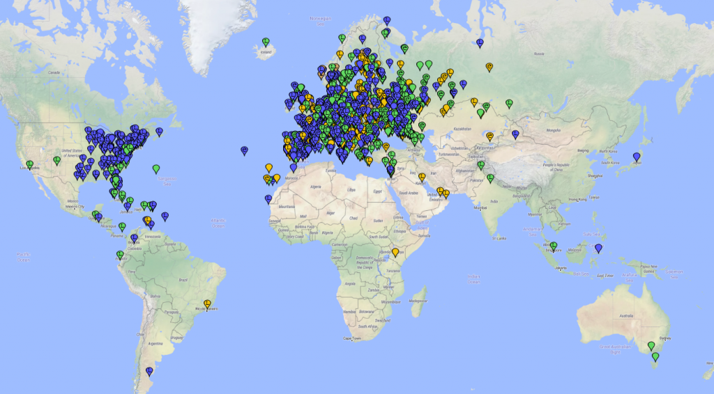
Since we know (at least to within 10km) where a transmitting station is, it becomes possible to plot the stations on a map. You’ve probably seen this done before. Websites like PSKReporter and WSPRnet have been doing this for some time now.
The image above use different coloured markers for different bands:
Marker Colour
Band
Blue
40m (7074 kHz)
Green
30m (10136 kHz)
Yellow
20m (14070 kHz)
Brown
15m (21074 kHz)
I have been recently enjoying the ability to use the same untuned vertical antenna with the same radio on different bands simultaneously (the HL2 lets you remove any band-pass filtering). This allows you to see, for example, that while 40m was good for working Germany, 30m had good propagation into Australia.
PSKReporter lets you filter by mode, band, and time, so you can see what times a given band is open to a specific location. Excellent for helping to fill those missing DXCC slots you may have.
It was interesting for me to see that much of the more remote stations were received on the lower bands, 40 and 30m, and not 20m as I would have expected:
VK7BO at 6:06 UTC on 30m
VK3ZH at 6:33 UTC on 30m
K6SY at 5:28 UTC on 30m
LU1WFU at 1:50 UTC on 40m
YE8QR at 14:46 UTC on 40m
Although at the time of writing (August 2020), HF conditions are quite poor, not all of the lack of performance on 20m can be explained due to the band conditions, since 20m is still open to South America and into Asia.
Animating the propagation
After looking at these static images, I wanted to see how things changed with time. Could I, for example, see when the best time to work the west cost of the USA would be? I decided to make a time-lapse animation. The animation runs for approximately 3 days, and includes the following FT8 decodes:
Band
Decodes
40m (7074 kHz)
72,404
30m (10136 kHz)
33,871
20m (14070 kHz)
156,636
15m (21074 kHz)
3,453
It is clear to see sudden bursts of colour when a band opens, and to watch conditions change throughout the day. The dates here were for a Friday to Monday, so, there’s plenty of weekend activity.
I’m keen to further explore the possibilities of this.
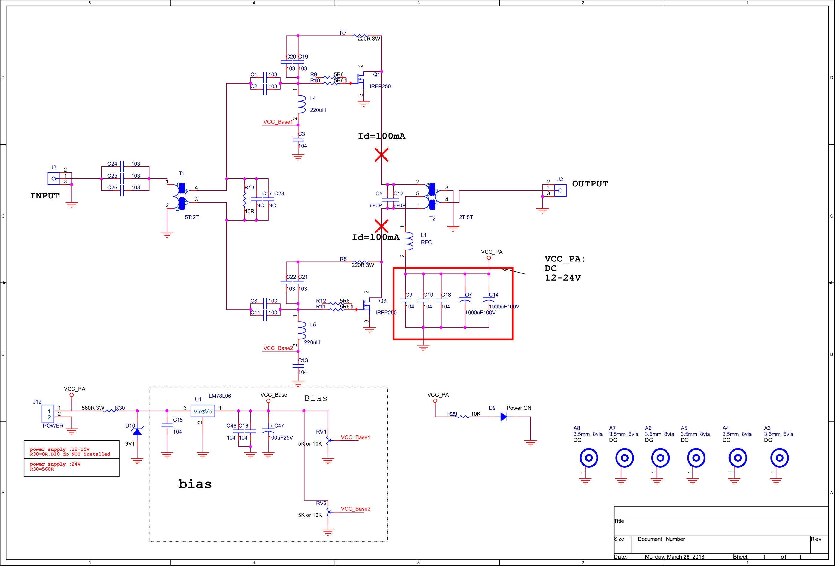
This page is about the Chinese RF_PA_250_3_HV_V201 by ZGJ 2018-01-25, version 201, commonly for sale on eBay, AliExpress, etc.
Sellers, you are welcome to link to this page in your listings.
This page is a mix of information from my own investigation as well as information found online (from several sources). It is useful for those purchasing kits for such amplifiers.
Click image to enlarge. For transformer winding information, see below.
Build Information
Version History
V100 – First edition
V101 – Second edition: Output transformer cores reduced to 14.
V201 – Third edition: Power supply voltage is raised to 24V.
What you will need
13.8V/24V 40A (or higher) power supply. It is better to have the function of current‐limiting protection. 6 square-mm (or more) wires for connecting the power to the amplifier board.
A signal source that is capable of outputting a 7 or 14 MHz signal at 10W.
A 50Ω dummy load rated for 200W (must be able to withstand continuous dissipation).
A heatsink suitable to dissipate the power of Q1 and Q3. (Recommended size: no less than 150x100x60mm).
A multi-meter that includes a 10A scale.
An oscilloscope capable of at least 20 MHz (or a spectrum analyser).
Before you start soldering
Wind the inductor (L1) and transformers (T1 and T2) in accordance with the information further on in this page.
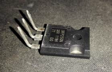
Bend the legs on Q1 and Q3 (TO247 package) upwards, see the illustration below. Do not mount it to the top side of the board. Do not shorten the leads.
Tap the holes for Q1 and Q3. Screw should be M3 (3mm screw). Clean the heatsink, and remove any metal chips to avoid a short circuit.
Soldering
Start with smaller components first, working up towards larger components and finally plugs.
SMT parts can be easily soldered with an iron by adding a small amount of solder to one pad, and using tweezers to push the SMT part into the molten solder on the pad. Once cooled, add a small amount of solder to the other pads.
L1 and C5/C12 are not fitted at this stage.
Preparation for Powering
Check for any solder splashes, and poor or missing solder joints.
Check the DC power supply resistance to ground – no short circuits. If you have not fitted L1 yet, test from the other side of L1 pad.
(Note: in the V201 version, there are 14 cores in the output transformer, not 16 as shown here)
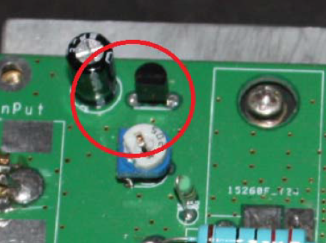
Check the LM78L06 regulator output resistance to ground – no short circuits.
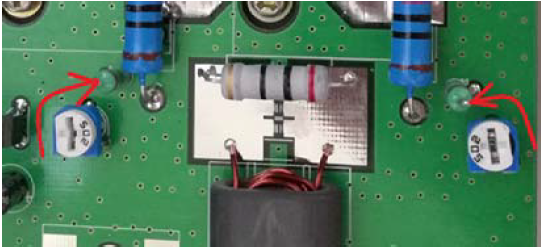
Check the bias-set variable resistors. Rotate them as shown in the following diagram. Be careful, to rotate them to the correct end-stop. If you get this wrong, you will destroy the IRFP250N power MOSFETs. You are aiming for an initial bias voltage of 0V.
Mount the input transformer secondary load resistor (10Ω, 3W).
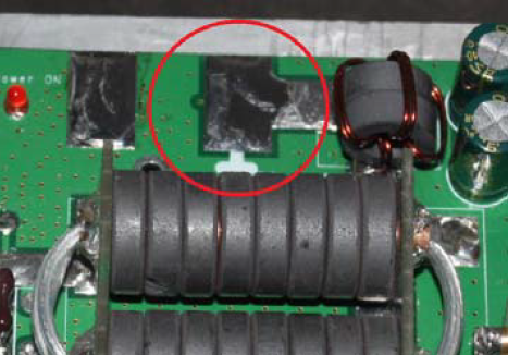
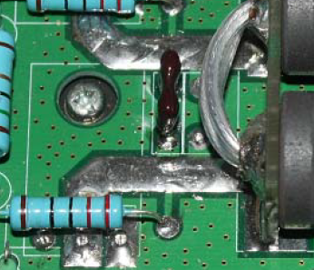
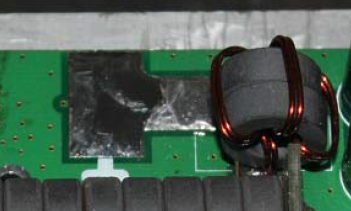
Solder in Q1 and Q3 and affix to the heatsink. Flow solder on the PCB trace between the MOSFET and the output transformer. This increases the current capacity of the track. See below.
Mount L1 as shown below.
Set bias currents
The aim of this section is to adjust the bias current to 100mA for each of the two transistors. When making adjustments, you must act slowly, and with great care – the current will do nothing for much of the adjustment range and then rise sharply. The transistors must be bolted to a heatsink during adjustment.
Double-check that the variable resistors are ‘zeroed’ as described above, such that when power is initially applied, there is no bias voltage present.
Connect a current meter in series with the positive power supply cable of the amplifier. Apply power.
Adjust the upper MOSFET quiescent (static) current using the upper variable resistor to cause an increase in current of 100mA (0.1A).
As before, now adjust the quiescent current of the lower MOSFET to further increase the current another 100mA. (A total increase of 200mA between both transistors.)
Solder in choke inductor L1 and mica capacitor C5/C12 if you have not already done so – the bias adjustment is complete.
Signal test
Connect a 50Ω dummy load to J2. The load must be capable of handling 200W.
Use an oscilloscope on a suitable range (or spectrum analyser with suitable attenuation) to monitor the signal at the load.
Connect the power supply and monitor the supply current for a moment. If the current is gradually increasing, the power must be cut immediately and check for suitable thermal connection between the power transistors Q1 and Q3 and the heatsink.
With the amplifier powered and no input, check the oscilloscope for signals. If there signals, immediately power off and debug the cause of self oscillation.
Input a small signal, gradually increasing the input signal power.
Observe the output waveform and the DC input current. In general, 100Vpp output across the output load corresponds to a power output of 25W into 50Ω. A load voltage of 141Vpp is 50W output, 180Vpp load voltage gives an output power of 80W, and 200Vpp at the load is a power output of 100W. Using an efficiency of 55% as an approximation, the expected DC power input can be calculated.
Check the temperature of the heatsink. If it is too hot to hold, then you will need to use a fan to cool the amplifier.
Check the output power is stable over time, and that there are no large fluctuations in output power for a fixed input power.
Finishing
Use a flux remover to clean any solder flux residue and tidy any poor solder joints.
Mount the amplifier into a box or case with suitable TX/RX switching.
Accompany the amplifier with a suitable low-pass filter board.
Transformer & Coil Winding
In the following diagrams process, please note:
To avoid scraping the enamelled wire, use needle nose pliers to smooth the edge of the ferrites. Hole edges may be sharp.
A “turn” on the coil is regarded as wire passing through the centre.
Winding T1
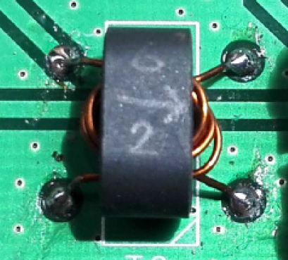
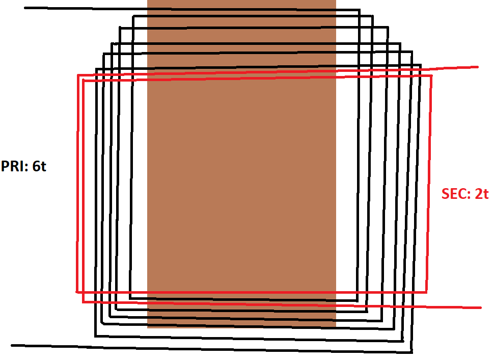
Transformer T1 primary should be 6 turns (black lines). The secondary of T1 should be 2 turns (red lines). The turns ratio is important, since if there are too many turns, the voltage on the gates of the MOSFETs will exceed the breakdown voltage and the parts will be destroyed.
Winding T2
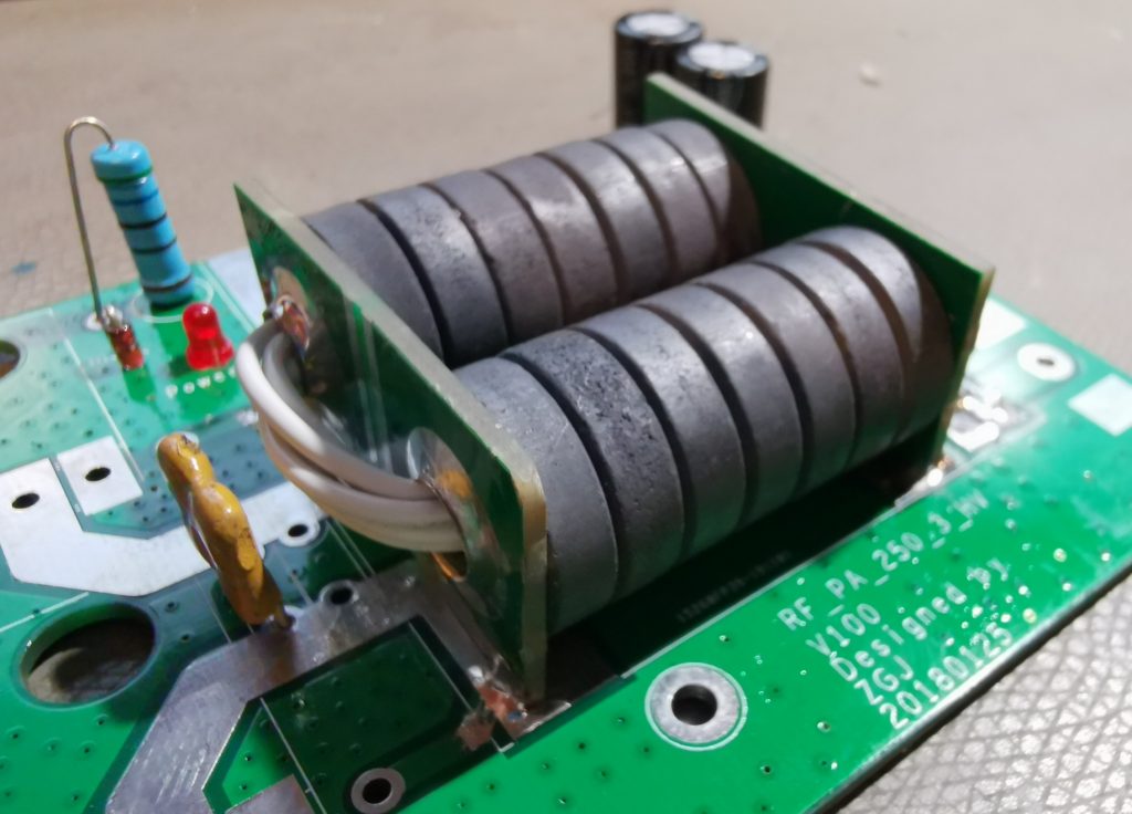
Transformer T2 primary should be 1 turn made from the two end PCBs and copper pipe. The secondary of T2 should be 5 turns of high temperature wire.
In version 201 of the kit, the number of ferrite rings is reduced from 16 to 14. You will also need 2 ferrites for winding L1 (see below).
Winding L1
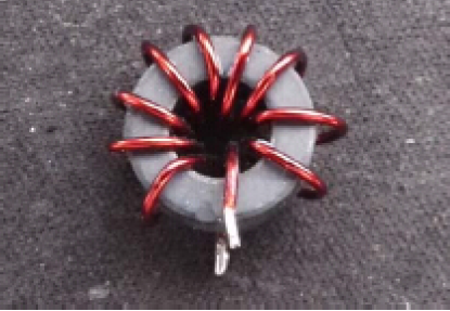
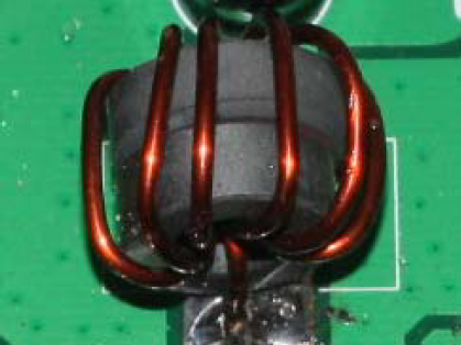
L1 is a high frequency RFC choke. The 7-10 turns should be wound around two ferrite rings as used in T2. I chose 10 turns as this provides the largest choke inductance.
I noticed after a while, that my BER percentage of my MMDVM_HS_Hat and Pi-Star setup was significantly higher than other users, at around 3.5%. I know from setting up GB7KH that getting this correct takes patience. I also happen to know that the design of the MMDVM_HS_Hat uses inexpensive TCXOs to provide frequency and timing references. As such, some calibration can do wonders for the BER on DMR.
For this mini-guide, I shall use my TYT MD-380 handheld DMR radio. My hotspot is set to use a nominal frequency of 434.250 MHz as the carrier frequency.
Using the DMR handheld as a transmitter on low power, it should be possible to better match the frequency of the receiver to the transmitter – this process isn’t ideal, because it could equally be the handheld frequency which is incorrect – but at least they’ll match.
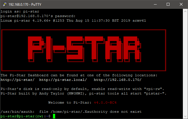
We’ll need to get SSH access to the underlying Linux system on the Pi-Star. You can either use the “SSH Access” tab from the Pi-Star Expert menu, as below:
Pi-Star SSH Access via Expert menu
Or you may prefer to SSH into the Pi-Star with your preferred SSH client – I use PuTTY. Either option will work here.
The program we need is called MMDVMCal. Fortunately, there’s a version compiled for us already in Pi-Star. From the Pi-Star console terminal, the following command will start the MMDVMCal program where we’ll do our testing:
$ sudo pistar-mmdvmcal
Using MMDVMCal
When the program starts, you’re greeted with the following command line instructions. You may also see some debug/warnings about
Starting Calibration… Version: 1, description: MMDVM_HS_Hat-v1.4.17 20190529 14.7456MHz ADF7021 FW by CA6JAU GitID #cc451c4 The commands are: H/h Display help Q/q Quit W/w Enable/disable modem debug messages E/e Enter frequency (current: 433000000 Hz) F Increase frequency f Decrease frequency Z/z Enter frequency step T Increase deviation t Decrease deviation P Increase RF power p Decrease RF power C/c Carrier Only Mode K/k Set FM Deviation Modes D/d DMR Deviation Mode (Adjust for 2.75Khz Deviation) M/m DMR Simplex 1031 Hz Test Pattern (CC1 ID1 TG9) K/k BER Test Mode (FEC) for D-Star b BER Test Mode (FEC) for DMR Simplex (CC1) B BER Test Mode (1031 Hz Test Pattern) for DMR Simplex (CC1 ID1 TG9) J BER Test Mode (FEC) for YSF j BER Test Mode (FEC) for P25 n BER Test Mode (FEC) for NXDN g POCSAG 600Hz Test Pattern S/s RSSI Mode I/i Interrupt Counter Mode V/v Display version of MMDVMCal <space> Toggle transmit
The first thing to do is to set the MMDVMCal frequency. I did this by pressing “E” followed by the frequency of my radio (434.250 MHz) in Hz.
e
434250000
You should see this frequency echoed back in brackets once the menu is reprinted to the screen. If you look at the example above, you’ll see that the frequency is 433000000 Hz (or 433.000 MHz). Pressing “b” will enter “BER Test Mode (FEC) for DMR Simplex” mode:
b
At this point, a quick transmission will show the exact BER:
DMR voice header received DMR voice header received DMR voice header received DMR audio seq. 0, FEC BER % (errs): 2.837% (4/141) DMR audio seq. 1, FEC BER % (errs): 2.837% (4/141) DMR audio seq. 2, FEC BER % (errs): 3.546% (5/141) DMR audio seq. 3, FEC BER % (errs): 1.418% (2/141) DMR audio seq. 4, FEC BER % (errs): 0.709% (1/141) DMR audio seq. 5, FEC BER % (errs): 2.128% (3/141) DMR voice end received, total frames: 6, bits: 846, errors: 19, BER: 2.2459%
My BER is showing as 2.5%. Not awful, but with some room for improvement.
The process of finding the ‘perfect’ value is twofold. The first is to find the approximate frequency, and then dial in the exact value. Here, we’re trying to find out the difference between the nominal frequency (in my case 434.250 MHz) and the optimal working frequency.
From the menu above, you’ll note that both “F” and “f” (both upper and lower case) increase and decrease the frequency respectively. By holding your radio in transmit, repeatedly press the F key until you the MMDVM_HS_Hat looses the transmission from your handheld. You’ll see the TX frequency announced with each change of frequency – allow time between each step (around 10 seconds on each frequency).
Keep going in one direction until the software reports “Transmission Lost” – note the final frequency down. You can see this by pressing “H” or “h” to reprint the menu. For me, the first limit I reached was 434249800 Hz by repeatedly pressing “f” to lower the frequency.
From here, you can find the mean (centre) frequency: (434249800 + 434250800)/2 = 434250300 Hz (300Hz higher than the nominal).
Use the “E” command once again and enter your new mean frequency – for me, this was 434250300 Hz.
e
434250300
You can then either enter frequencies yourself stepping 10 Hz at a time until you find the frequency yielding the best BER, or you can use the “Z” and “z” commands to increase or decrease the steps, and continue using the “F” and “f” commands to ‘home in’ on the value. I tabulated my results to give me a clear understanding of what was going on. I first went with 25 Hz steps (half the default 50 Hz steps) and found the following values for a 15 second transmission on each frequency. At the end of each transmission, status (including BER) are reported. You can see that the optimum value was very close to my mean value.
You can see that the optimum value was very close to my mean value. I experimented with even smaller steps, but didn’t really improve much on the 0.1% BER. This value is definitely good enough, and is an order of magnitude better than what I had previously!
Since I also use D-STAR, I quickly pressed “K” to enter D-STAR BER test mode, and, with the best settings from DMR, I keyed my Kenwood TH-D74 handheld – everything was fine here, too:
D-Star audio FEC BER % (errs): 0.000% (0/48) D-Star audio FEC BER % (errs): 0.000% (0/48) D-Star audio FEC BER % (errs): 0.000% (0/48) D-Star audio FEC BER % (errs): 0.000% (0/48) D-Star audio FEC BER % (errs): 0.000% (0/48) D-Star audio FEC BER % (errs): 0.000% (0/48) D-Star voice end received, total frames: 214, bits: 10272, errors: 0, BER: 0.00000%
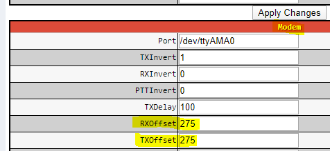
Taking the frequency for your lowest BER (in my case 434250275 Hz), the offset is easy to calculate: Simply subtract the best BER frequency from the nominal frequency to find the offset: 434250275 – 434250000 = 275 Hz (note, this can be negative).
Applying the Offset
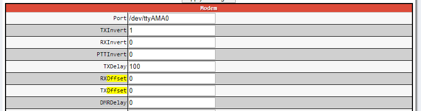
We next need to apply our offset (in my case +275 Hz) to the main MMDVMHost application running on the Pi-Star. This is done through the expert configuration.
Inside the Pi-Star configuration, head to the Admin Expert menu once again and select MMDVMHost.
Inserting our calculated offset (in Hertz) from the above.
With the outbreak of the novel coronavirus (COVID-19) in late 2019 and spreading through Europe early 2020, a lot of tech and IT media wrote to encouraging people to take up Folding at Home (FAH, F@H). I decided to join in, which for the most part was pretty easy, just a case of installing the software – more on this later. But on my larger PCs, I wanted to make use of my Nvidia GeForce GTX 1070. Using a GPU adds another workhorse to the project, and is often faster/more suited to some of the computation tasks (called Work Units or WU).
Installing the Software
The Folding at Home software comes in 3 parts: the client (FAHClient) which does the computation work; the controller (FAHControl) which provides a GUI for the client; and a viewer (FAHViewer) which renders pictures and illustrations of the molecules being computed, albeit at the expense of some compute performance.
The FAH Downloads Page has the files you need to get started. On Linux, you’ll need the following files:
The first line installs the package and the second will obtain any dependencies for the package. You may see errors after installing the first package, but after the second, you should have any dependencies met. You may need to tinker around and help the package manager fix any missing issues.
You’ll notice that I have supplied a modified version of FAHControl. This has one of the dependencies removed, which means it is possible to install on newer Ubuntu versions.
Once you have the programs installed, the client will start. You can stop and start it with:
$ sudo service FAHClient stop # stop the client
$ sudo service FAHClient start # start the client
You’re ready to go. Use the control program to make changes to settings, etc. You’re ready to start folding on your CPU!
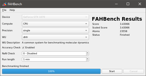
You may be interested to benchmark your machine with FAHBench. The process takes a little over a minute to run a 1 minute test, and it reports if everything is working correctly. Fror
Setting up the Nvidia GPU
The more tricky part, for me at least, was getting the environment set up for the Nvidia display.
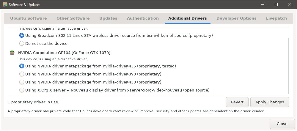
The first thing to do is to open the “Additional Drivers” dialogue box from the “Software and Updates” menu. You can jump directly to this by running the following in a terminal:
$ software-properties-gtk --open-tab=4
Typically, you should select the newest driver available. At the time of writing, “nvidia-driver-435”. If you are not running an X server and just want to install the driver without the requirement for X, you can install “nvidia-headless-435”. You may also care to install “nvidia-utils-435”.
After pressing Apply Changes, the system will download the latest drivers and install them with the required dependencies. We’ll add some extra packages of our own too:
You may also wish to tinker with the GPU a little bit, choosing to either underclock or overclock the GPU to get either better reliability or improved performance. One thing to note with overclocking is that while the occasional glitch or artefact is acceptable during gameplay, it will cause a FAH WU to fail.
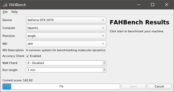
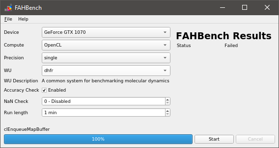
Initially with my configuration, I fount the factory overclock on my Asus ROG Strix GTX1070 O8G to be slightly unstable in FAHBench. I found that the GPU would fail at at between 7% and 9% of the way through the test.
GPU Benchmark Starts
GPU Benchmark Fails
Further investigation using the Unigine Superposition as a GPU stress test allowed me to tinker with the settings to find a reasonable GPU Core and Memory overclock parameters, as well as appropriate power limits. The Asus ROG Strix GTX1070 has good cooling and so I was able to get away with increasing the power limit and adjusting the clocks for long-term stability. Bear in mind that stability is way more important than getting that last couple of percent from the card.
Overclocking and tinkering was done using a mix of Green With Envy and the “nvidia-settings” tool on Xubuntu 19.10 which come with the driver and “nvidia-smi” which comes with the “nividia-utils-xxx” package.
Other Considerations
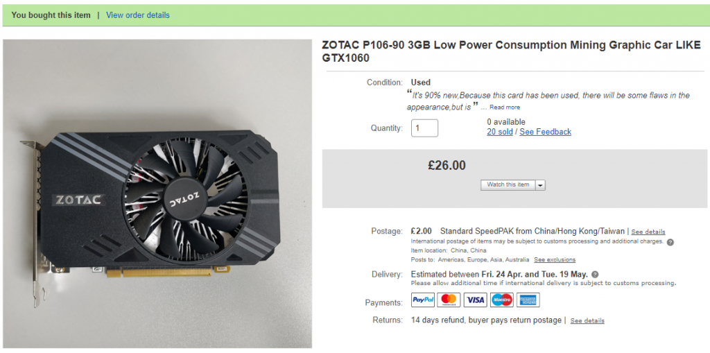
If you don’t fancy pushing your expensive graphics card hard, you may be able to find a custom GPU card previously used for mining crypto-currencies. These cards feature the same GPU chipsets, but are crippled such that they cannot easily (although it is possible) generate video. The Nvidia P106 offers features similar to the GTX 1060, while the Nvidia P104 offers features similar to the GTX 1070.
Since GPUs are no longer viable to generate crypto-currency, they’re often sold second hand on eBay and similar sites for relatively cheap prices. While a modest Nvidia GTX 1060 with 3GB of VRAM costs around £150 on eBay at the time of writing, an Nvidia P106-90 (GTX 1060 with 3GB VRAM) costs as little as £26 each or £20 in bulk! At a once off, that’s nearly a sixth the price.
Watch this space for an update on how these perform…
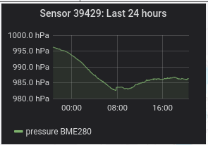
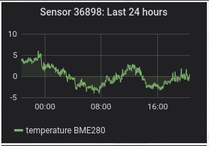
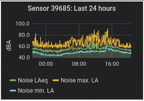
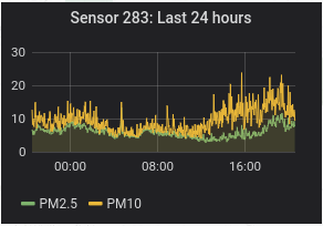
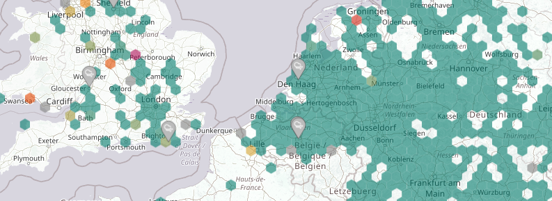
Around a year ago a colleague mentioned to me the Luftdaten project (en: air data project). It is a sort of citizen science project which measures and records particulate matter in the air. They also have a newer project concerning acoustic noise levels (build notes for this in German here), but I’ll be concentrating on particulate matter here. Often the sensors are combined to collect data on airborne particulate levels, acoustic noise, temperature, humidity and air pressure to name a few. The images below show 24h graphs for some of the measured parameters from various sensors around Europe.
Air pressure
Temperature
Acoustic noise
Particulate matter
I have long had a fondness for collecting data and the Luftdaten project has plenty! Their website features an interactive map of the world where they plot measurements taken.
The particulates detected include dust, dirt, soot, smoke, and liquid droplets emitted into the air which are small enough to be suspended in the atmosphere. Airborne particulates may be a complex mixture of organic and inorganic substances. The type of sensor used does not differentiate between the particle types, it just gives a measure of how many are present.
Parts
I purchased all of the parts cheaply from AliExpress (no affiliation). You’ll find the same parts on eBay, BangGood, etc., so use what you prefer.
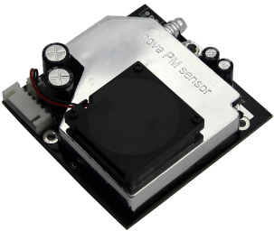
The particulate matter sensor is a Nova SDS011 PM sensor (datasheet), which can be purchased for around £14.
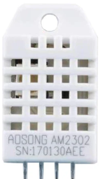
You’ll probably also want a DHT22 temperature & humidity sensor (datasheet) which will cost around £2.
Finally a NodeMCU V3 is required. This is a module based on the ESP8622 WiFi chip, which includes a USB-UART interface, some voltage regulators, etc. In a later step, we’ll program this with the Luftdaten code.
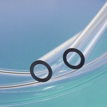
A short length of plastic pipe can help to draw air into the SDS011 sensor. The datasheet for the SDS011 suggests an inside diameter of 6mm and outside diameter of 8mm.
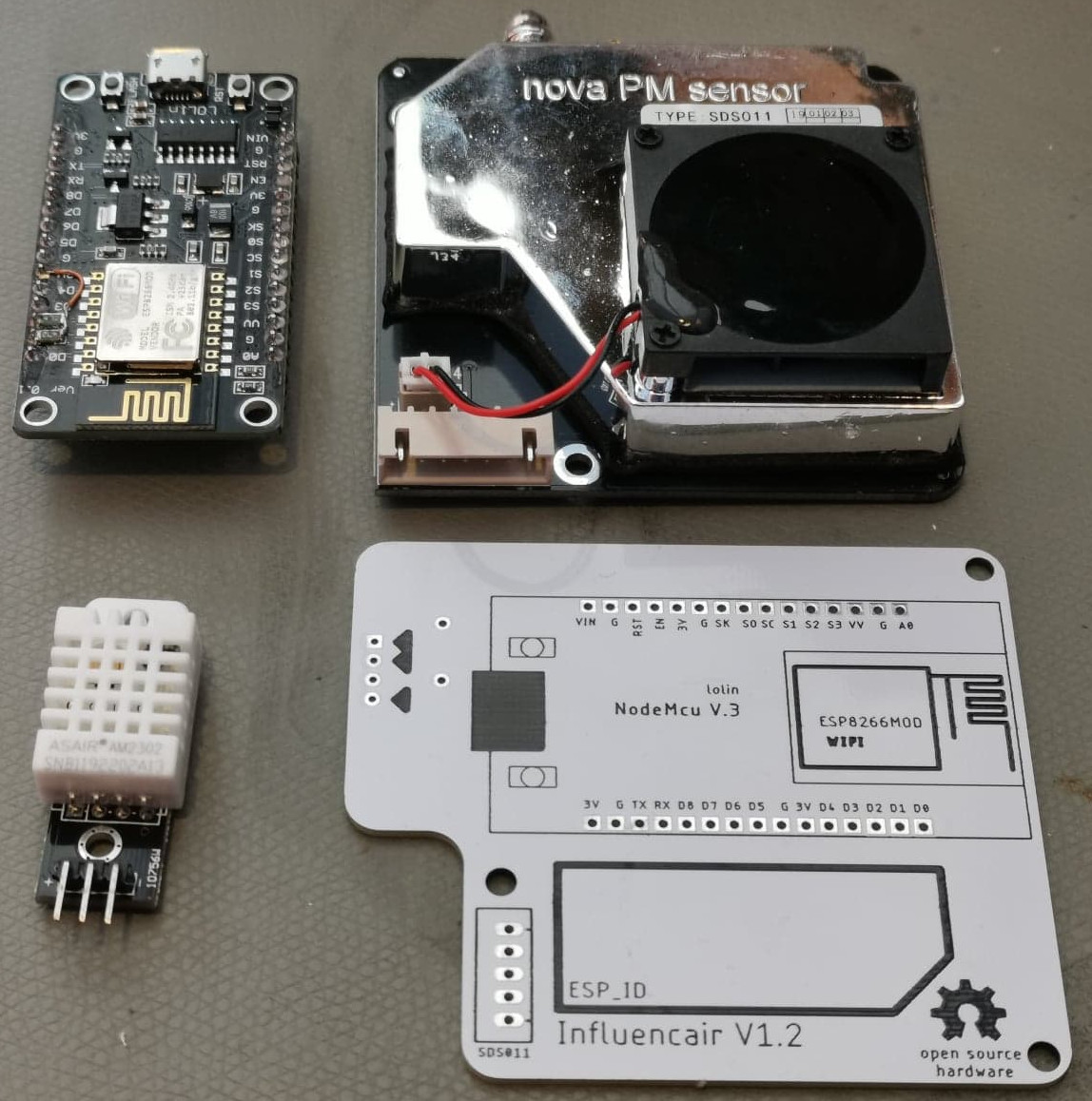
The photo below shows my assembled parts! You’ll notice int he bottom right of the image that I have an Influencair V1.2 PCB. Influencair are a spin-off group of Luftdaten based in Belgium. CivicLabsBelgium produced PCBs for project participants to use and made the PCB Gerber Files available here. You can send these off for manufacture using any PCB service you like (for example, in no order JLCPCB, PCBWay, DirtyPCBs, Elecrow, and so on).
Build notes & Programming
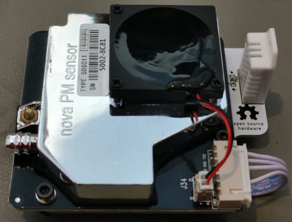
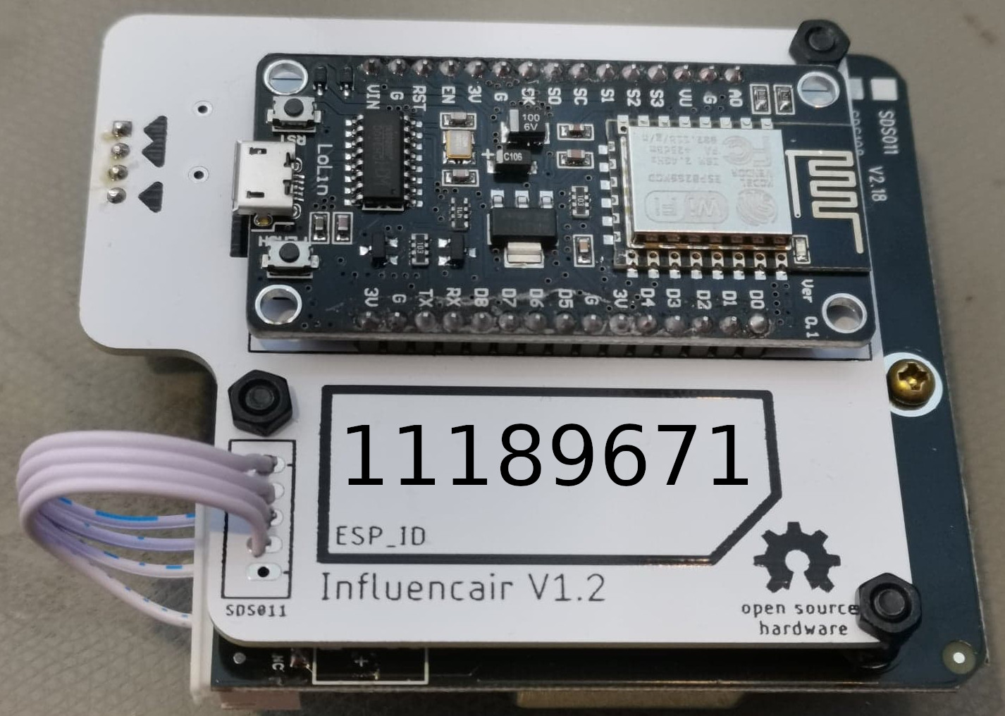
The build process is explained thoroughly on the Luftdaten website under the construction manual page. As I won’t be able to do a better job of explaining this, I suggest you go ahead and read their documentation. Below shows the parts mounted on my Influencair V1.2 PCB. I used 3mm screws to hold everything together.
Programming, Configuration & Registering
The default programming proceedure requires setting up the ESP8622 in the Arduino software environment, but Piotr Dobrowolski has created a very useful tool: airrohr-firmware-flasher for the Luftdaten project. I used the Linux variant of the program the NodeMCU in one click, but Windows and macOS versions exist too! Be sure to find the “releases” button on GitHub to download the pre-compiled ready-to-use binaries!
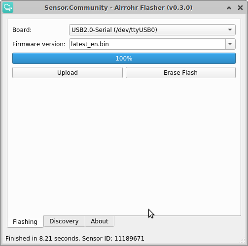
With the NodeMCU connected to the PC with a USB cable, I selected “latest_en.bin” from the version list (en being English), and pressed Upload. As you can see from the figure below, it took just over 8 seconds and it was done!
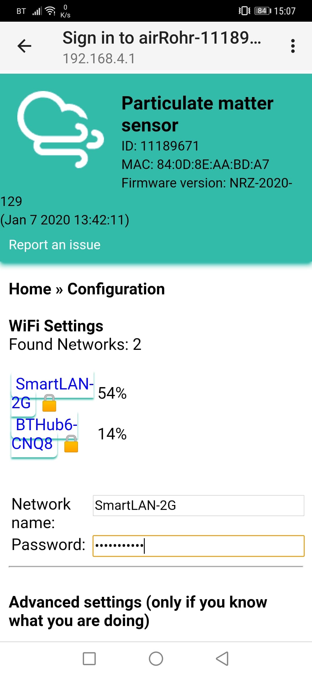
Power cycling the board resulted in a WiFi device being created by the newly created sensor! I connected my mobile phone to “airRohr-11189671” and was greeted with the following screen.
I tapped on my house WiFi “SmartLAN”, entered my super-secret passkey and we were away! The device power cycled and was then visible from the flasher once again.
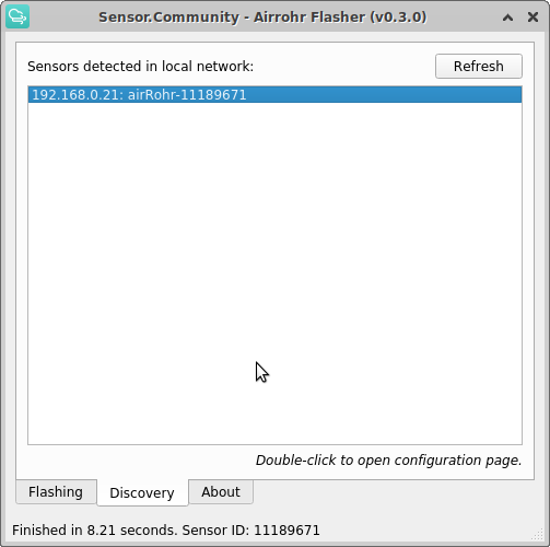
From this, I was able to see the sensor was assigned an IP address on my network, and double-clicking on the entry whisked me off to my default web browser viewing the sensor’s internal webpages.
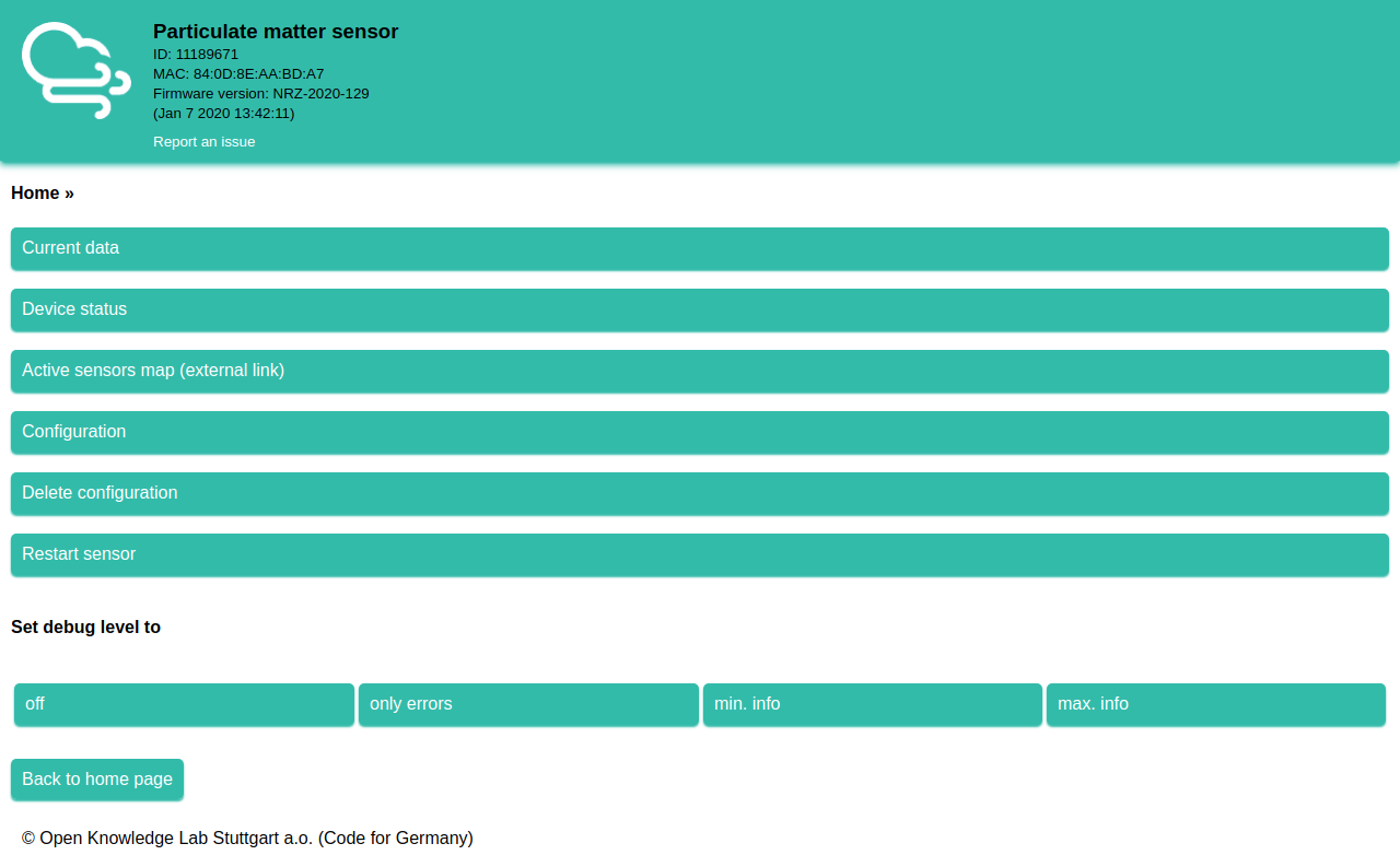
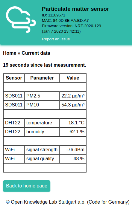
There are many configuration options, but the defaults were suitable for my hardware configuration. There are options for OLED and LCD screens, extra/different sensors and many other configurations which are out of the scope of this article. However you can click “Current Data” to see the sensors latest measurement data. The image below was taken with the sensor indoors.
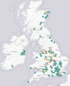
The final thing to do is to create an account on the Luftdaten project website so your sensor can contribute measurements. There are already a reasonable number of sensors in the UK contributing data to Luftdaten. You can create your account and submit your sensor data here: https://meine.luftdaten.info
I have positioned my sensor in the garden shed with a short section of plastic pipe poking outside of the shed where the wind blows. I live near a busy roundabout and buy a petrol filling station, so it will be interesting to compare my measurements with other local sensor readings.
Over the past few evenings, I have been experimenting with phase-frequency detectors. I have an upcoming project that requires the use of one, and, I figured I’d refresh my memory on them. I ended up using my Lattice MachXO2 breakout board as the development platform.
The first step was to divide a 10 MHz crystal oscillator down to 10 kHz. That was easily done with a counter, counting from 0 to 499, and then resetting to 0. Every reset would simultaneously toggle an output bit, with the net result being a square-wave clock on the output bit, periodic every 1000 cycles of the input. A divide by 1000 counter.
Next was to understand the Phase-Frequency Detector (PFD). This is commonly referred to as a Type 2 detector, since it detects not only phase difference but frequency difference. This means that the PLL will only ever lock to the fundamental frequency, and not harmonics. It also means that when the loop is unlocked, the PFD knows which way to drive the VCO to regain lock. A Type 1 detector only uses phase information, and so drives the oscillator in the direction of the phase difference until the loop locks – as a result, Type 2 detectors lock quicker.
The Type 2 detector has two outputs, up and down, which pulse for the required direction with a duty cycle proportional to the phase difference.
I spent a few days designing and simulating the PFD using the Aldec Active-HDL simulator to confirm that my circuit did indeed perform as expected:
I then added a simple lock detector, which set a locked signal high if the phases were in lock for the past 10 cycles as a proof of concept. In reality, a much longer observation window will be used. It is possible to see the lock signal becomes high after 10 cycles.
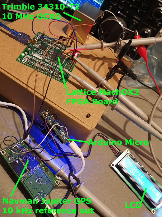
The final stage of this project snippet was to test on real hardware. The Verilog code was pushed through synthesis, place and route, and a configuration file for the Lattice FPGA generated. This was then programmed into the board, and the board taken to the lab – you can see all the main parts of the setup in the photo below.
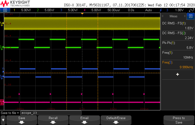
Below, you can see the scope traces from the probes in the lab bench photo. The yellow trace shows the 10 MHz VCO frequency from the Trimble 34310-T2 OCXO. The green trace is a debug from the FPGA output showing the 10 MHz signal divided down 10 kHz. The blue trace is GPS locked 10 kHz reference output. Finally, the purple is phase detector output, here from the ‘down’ output of the detector since we see that the divided VCO output (green) slightly leads the GPS reference (blue). The ‘up’ output is at logic-0 throughout.
The next part of the project was to create the charge pump circuit which converts the ‘up’ and ‘down’ pulsed signals into an analogue control voltage for the VCO.
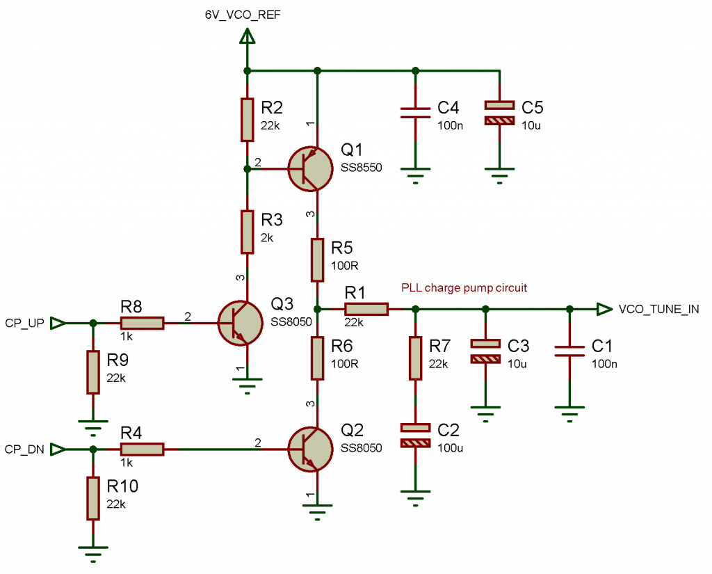
The parts for the charge pump took a few days to arrive, and while waiting I contrived the following circuit. Since the OCXO generates a 6V reference voltage for use with the VCO input (actually 5.4V in my case), it seemed wise to use that. Some crude experiments had lead me to a tune voltage of around 3.5V. The circuit uses a PNP transistor (Q1) to put pulses of energy into the filter network via R1. Similarly, it uses an NPN transistor (Q2) to remove pulses of energy from the filter via R1. R5 and R6 serve as a current limit in case both Q1 and Q2 are both powered. A further NPN transistor (Q3) acts as a voltage interface between the ~6V on the base of Q1 and the FPGA IO at 3V3 maximum. Only the values of components in the filter section are critical (R1, R7, C1, C2, C3); the others were chosen from what I had laying around.
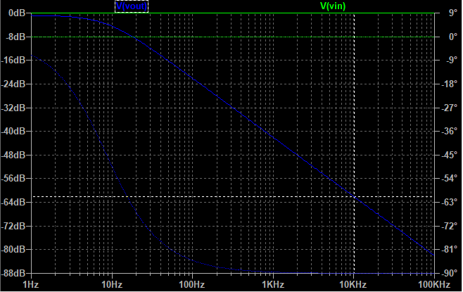
The loop filter was tested and tweaked in LTspice using the values above. The loop filter has around 62 dB of attenuation at 10 kHz (our reference [and thus up/down pulse] frequency).
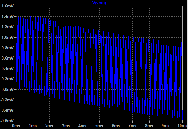
A look in the time domain shows we can expect about 1.5mVp-p at 10 kHz from visual estimation. An output of 1.5mVp-p is approximately 0.53 mVrms, which gives us around -66 dBV of attenuation (similar to we saw above). The curve of the waveform is the DC levels settling out at the start of the simulation.
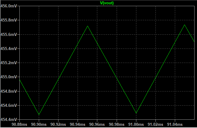
And finally the steady-state ripple; for a 1V square wave (0V-1V) input, a 1.23 mV ripple exists at the output (455.719-454.486).
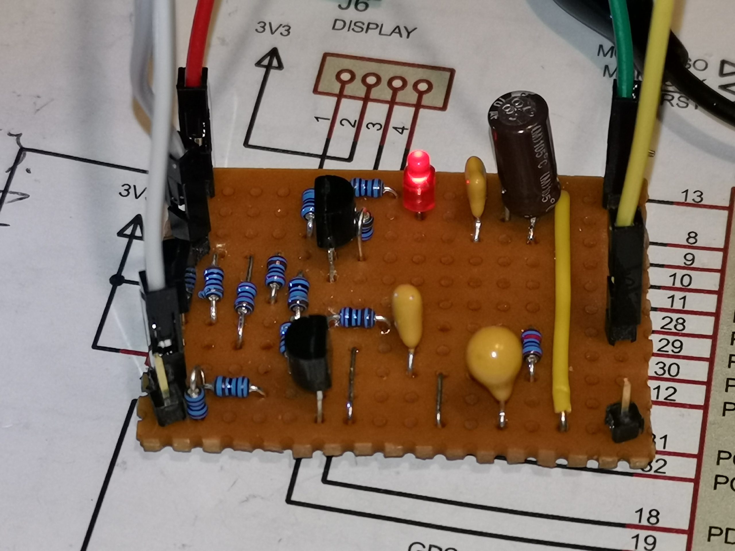
The penultimate step was to build the circuit and confirm it worked in real life. I made the charge pump on a scrap of strip-board, with pin headers for the main signals. On the left, +6V VCO reference input, the up and down signals from the FPGA, and on the right, ground and the VCO tuning input. The circuit is pretty much laid out as per the schematic, with the addition of an LED.
The final step was to watch the PLL lock on the scope! In the short video clip below, you can see the yellow trace is the 10 kHz reference frequency from the GPS. The green trace is the 10 MHz from the VCO. The blue trace is the 10 MHz divided down to 10 kHz. The purple trace is the VCO tune voltage – the output of the charge pump.
Recently lots of projects have been starting and ending in the background, but they haven’t made it to the website – despite some of them featuring on my Twitter feed.
I’m planning to spend a bit of time updating the website with current projects!
An online scrapbook full of half-baked projects and silly ideas.