As I was unable to take part in the CQWW CW Contest 2020 due to Coronavirus COVID-19 regulations, I decided to experiment with using the wideband SDR of the Hermes Lite 2 SDR (HL2).
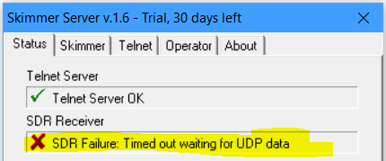
The process appeared to be quite smooth, however upon completion, the CW Skimmer’s Skim Server (SkimSrv) would report that the SDR connection had timed out. This transpired to be the hardware watch dog timer (WDT) timeout inside the FPGA on the Hermes Lite 2 – a precaution to stop the SDR from being stuck in transmit should the connection to it drop:
The solution was two-fold:
- Update the HL2 gateware to a version allowing the WDT to be adjusted/disabled
- Update the SkimSrv DLL plugin to a version using the WDT configuration
Getting the Latest HL2 Gateware
The gateware of the HL2 is a bit like what you may consider as firmware. Only, firmware is code that runs on a CPU or microcontroller, and gateware is code that configures the internal connections of an FPGA. This difference is immaterial here, but it is useful to know.
There are many versions of gateware available for the Hermes Lite 2. You are best advised to hunt around Steve Haynal KF7O’s project repositories for the Hermes-Lite2 under the gateware\bitfiles folder and find a version that best suits your needs. It is important to note that some of the gateware files in these folders are compiled with special features and are often not recommended for general use. Here I will cover two versions that I find interesting. The first is the standard gateware that supports both transmit and receive on 4 slices. The second receive only gateware swaps the transmit logic for extra receive logic, resulting in 10 receive-only slices.
One final note, the links I provide are for Hermes-Lite 2.0 build5 and later. If you have an earlier build, then there are different files required which are also present in the variants folders.
Standard 4-slice TX/RX gateware
I started off by finding the latest “testing” version of the HL2 gateware, which can be found in the repositories mentioned above. At the time of writing the original article “testing/20201107_72p5” was the latest version that was recommended for more general use. Since the original publication of this post, this has been rolled into the stable/20201212_72p8 release.
Once you have read the readme and are happy with the notes supplied with the version of the bitfile (the actual compiled file the FPGA is sent to configure itself), then you are ready to go.
Use stable/20201212_72p8/hl2b5up_main/hl2b5up_main.rbf (direct link to download) which supports up to 4 receiver slices, but also includes transmit and is suitable for general use – again – read the notes that are supplied! They are important. Whatever you chose, you may need to rename the “.rbf” file to “hl2b5up_main.rbf” to allow it to be flashed by SparkSDR. Quisk doesn’t seem to care what the file is called.
No transmit 10-slice receive gateware
My actual reason for changing the gateware was to try the 10-slice receive gateware for use with SparkSDR as a grabber for CW Skimmer, as well as all of the other digital modes (RTTY, PSK, WSPR, FT8, JT65, etc.).
For this, stable/20201212_72p8/variants/hl2b5up_cicrx/hl2b5up_cicrx.rbf (direct link to download) which supports 10 receiver slices but does not include transmit. This is meant for multiband skimmers.
Programming the Gateware
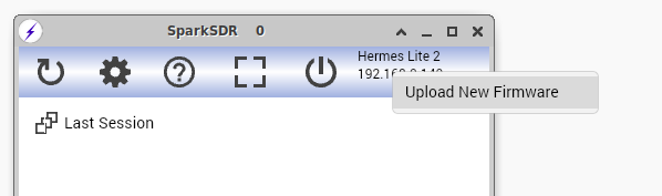
To program the gateware there are two options. I opted to use SparkSDR2 by Alan Hopper M0NNB. The process is easy and SparkSDR2 supports Windows and Linux. Run SparkSDR, press the discovery button (the rotating arrow on the left) until your Hermes Lite 2 is discovered, and then right-click and select firmware. From there, navigate from the downloaded and renamed file “hl2b5up_main.rbf” and press program. It should take around a minute.
You are also able to use Quisk by James Ahlstrom N2ADR. From the Config dialogue, select your radio, and then select “Program from RBF file”. The update should not take long.
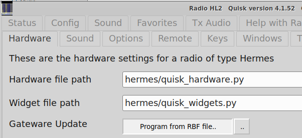
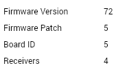
Once the upload is complete, you should power cycle the Hermes Lite 2 SDR, and then check in your favourite program that the update was successful. I checked that the radio still worked, and I could see that the revision gateware had changed to what I expected within SparkSDR: “Version 72 Patch 5” (now superseded by stable 72p8) and that I did indeed have 4 receivers available. If you used a different gateware version, you should see different results here:
Installing the recompiled HermesIntf.dll
Originally, the HermesIntf.dll file was provided by Vasiliy Gokoyev K3IT on the GitHub page HermesIntf. However, this DLL does not take advantage of the extra WDT options available in the HL2 gateware we just updated. To make such updates, this required the original DLL supplied by Vasiliy K3IT to be recompiled, incorporating changes from Steve KF7O’s gateware.
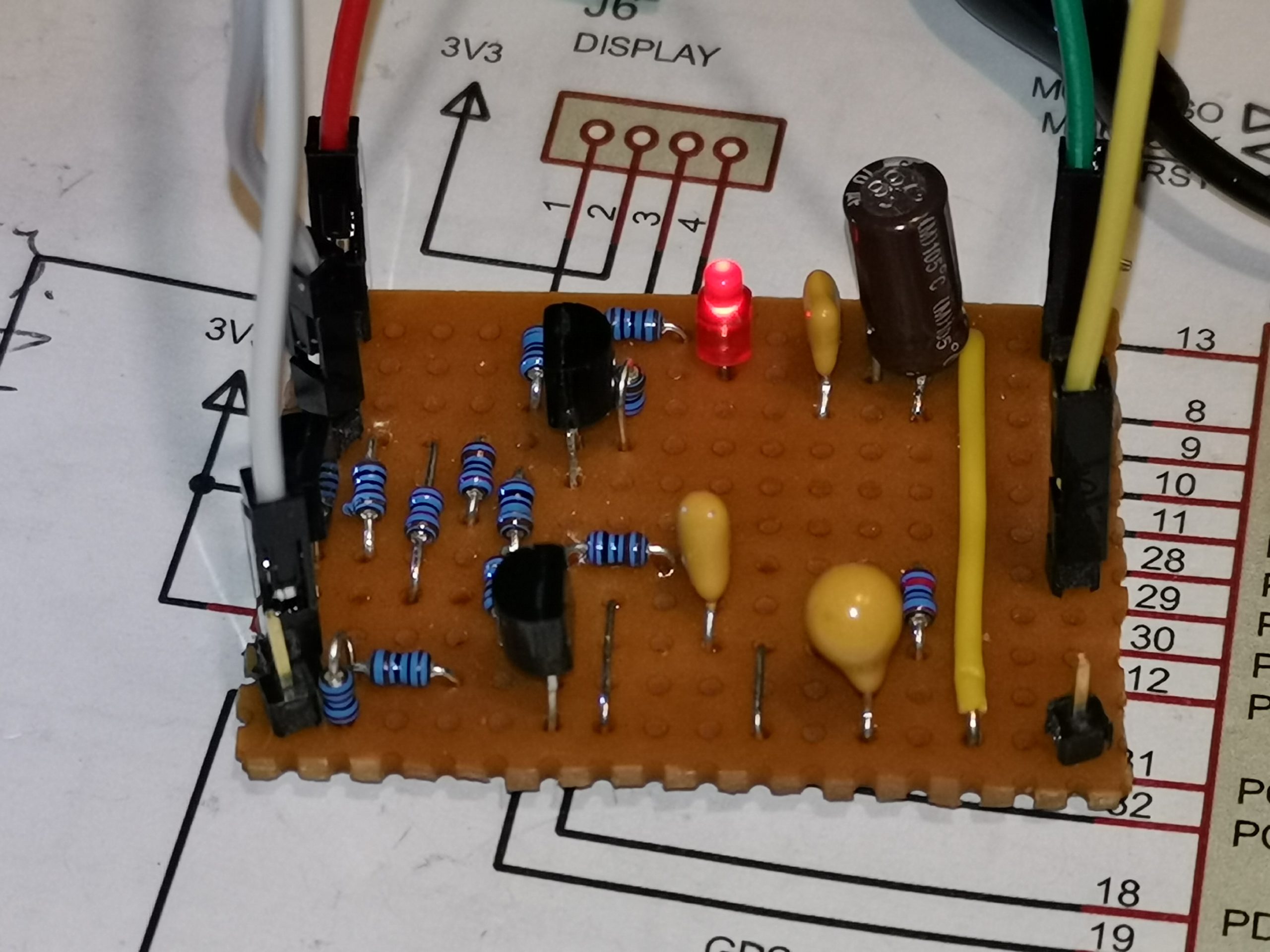
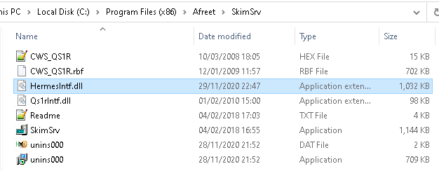
I was beaten to doing this by Robin Davies G7VKQ, who kindly shared the rebuilt DLL file with me on Twitter (thanks!!). This DLL file can be downloaded here: HermesIntf_G7VKQ.zip. There’s also a version by KV4TT (released Jan 2021) which I would suggest using as it has some further tweaks for handling the watchdog timer. This file is then to be copied into the SkimSrv folder, typically located within “C:\Program Files (x86)\Afreet\SkimSrv\” on a modern 64-bit version of Windows. You will of course need to install SkimSrv by Afreet Software from here. A trial version is available – you’ll need the Skim Server, not the standard CW Skimmer.
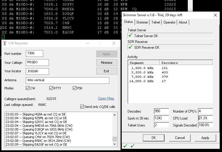
Once you’ve copied the DLL into the installation folder, you are ready to fire-up the SkimSrv. SkimSrv has a little icon in the system tray, as shown below. Click on this to open the SkimSrv settings dialogue.

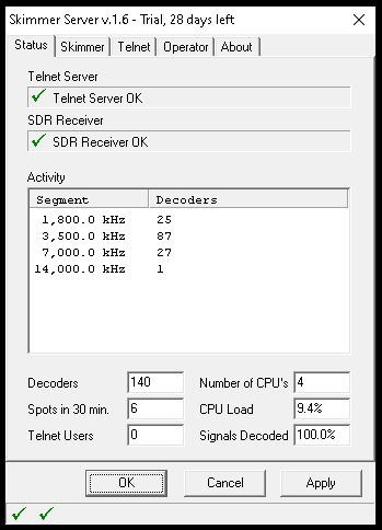
From here, you can use the Skimmer tab to set up the frequencies, sample rates, radios, etc., to use. This is all as you would expect and is pretty straight forward. Above, you can see I am using the 4 receivers available in the gateware version of the HL2 I chose. The image at the top of the page shows operation during CQWW CW 2020, where there were huge numbers of signals present on the bands.
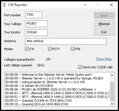
You can connect a telnet program to “localhost” on port “7300” to connect to the Skimmer Server by default. This acts like a DX Cluster with spotting information.
Uploading to PSKReporter
One of the most easy way is use CW Reporter by Philip Gladstone N1DQ. Philip runs PSKReporter, and, offers the CW Reporter application to interface between CW Skimmer Server and PSKReporter. It is easy to set up, working almost out of the box, and translates the DX Cluster style Telnet spots into reports for PSKReporter.info.
One comment to note here is that you should have calibrated your receiver’s frequency before doing this – otherwise, you may be spreading incorrect frequency information.
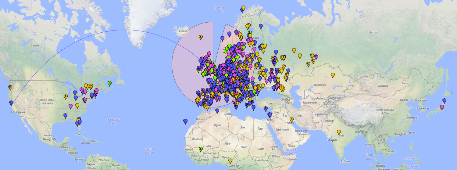
Finally, it is possible to see, on a map, using appropriate filters, what stations I have heard on CW over the past 24 hours:
Click any image to enlarge.
Thanks to everyone who offered help and suggestions along the way!