
This page details my building of Carlo Gnaccarini (VK3PY, formerly VK3BRZ)’s 100 Watt Power Amplifier for the 432 MHz Band based on two Motorola MRF646 transistors. Initially the information was obtained from Eugenio Martinetti (IT9VKY)’s site. The amplifier was straight forward to build. Some foolish mistakes (detailed later) prevented it from working immediately but a few emails with Carlo (Chas) quickly had the amplifier up and running. A few optimisations later and I was way!
I added some relay change-over circuits and make a few measurements and arrived at the amplifier presented on this page.
This project is in no way my design or work. It is entirely the work of those stated above. I offer this page as my experience in building their design!
The Design
The original article uses Motorola MRF646 transistors. I managed to salvage two from old PMR equipment, but some quick searching shows the following transistors may also be suitable. I cannot guarantee these, and so you are urged to check yourself.
- MRF646 (recommended)
- NTE367
- 2SC2905
- ULBM45
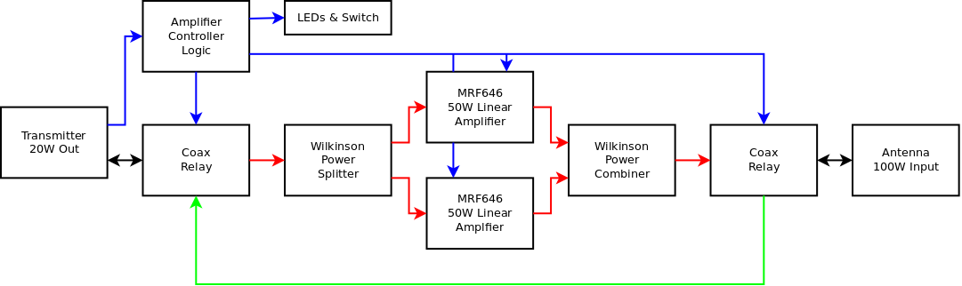
The design uses two transistors running as separate amplifiers (not push-pull). Each transistor is delivering half the power of the amplifier. Wilkinson Power Dividers/Combiners are then used to split the input through both halves of the amplifier and then rejoin the output. This is done in microstrip on the PCB. For a thorough explanation of the theory behind Wilkinson hybrids, see Ham Radio, January 1982, âWilkinson Hybridsâ by Ernie Franke WA2EWT.
Using two discrete amplifiers and matching networks as opposed to push-pull pairs has some advantages:
- No requirement for matched transistor pairs which eliminates crossover distortion issues.
- Good port isolation. If one transistor pops, the other should survive.
- Ease of design: “The Wilkinsons were the easiest way to obtain 100W without totally re-calculating all the matching networks (a very time-consuming job!)”.
- The two seperate amplifiers can be tested independently, fixed, debugged, tested, and then connected to the combiner.
The board also contains the biasing circuit for each transistor. These can be set up independently to aid unmatched transistors.
IT9VKY claims that the amplifier construction is very repeatable and I completely agree. I have built two of these boards and both performed very well.
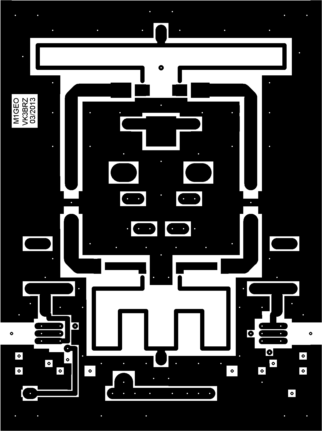
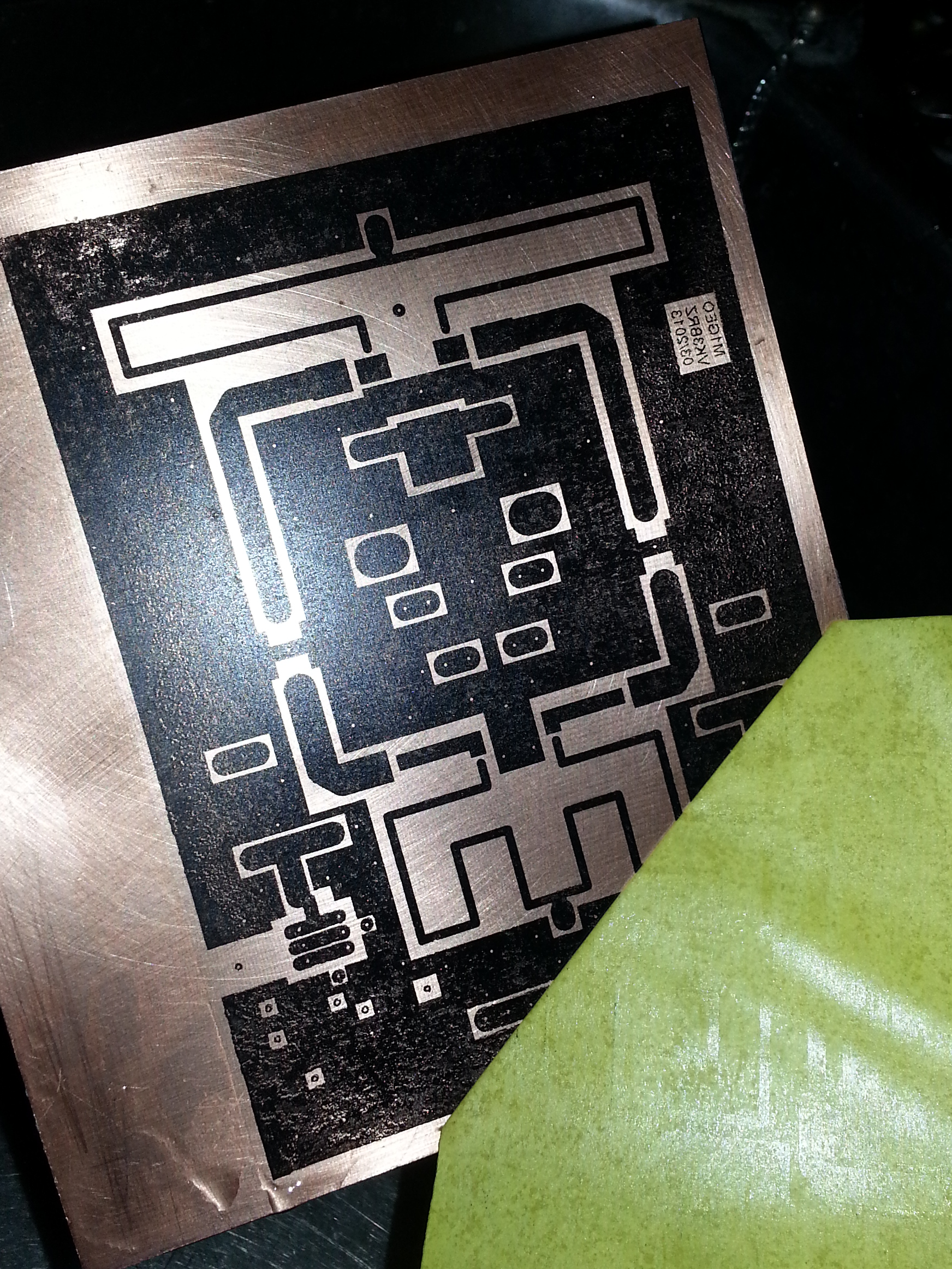
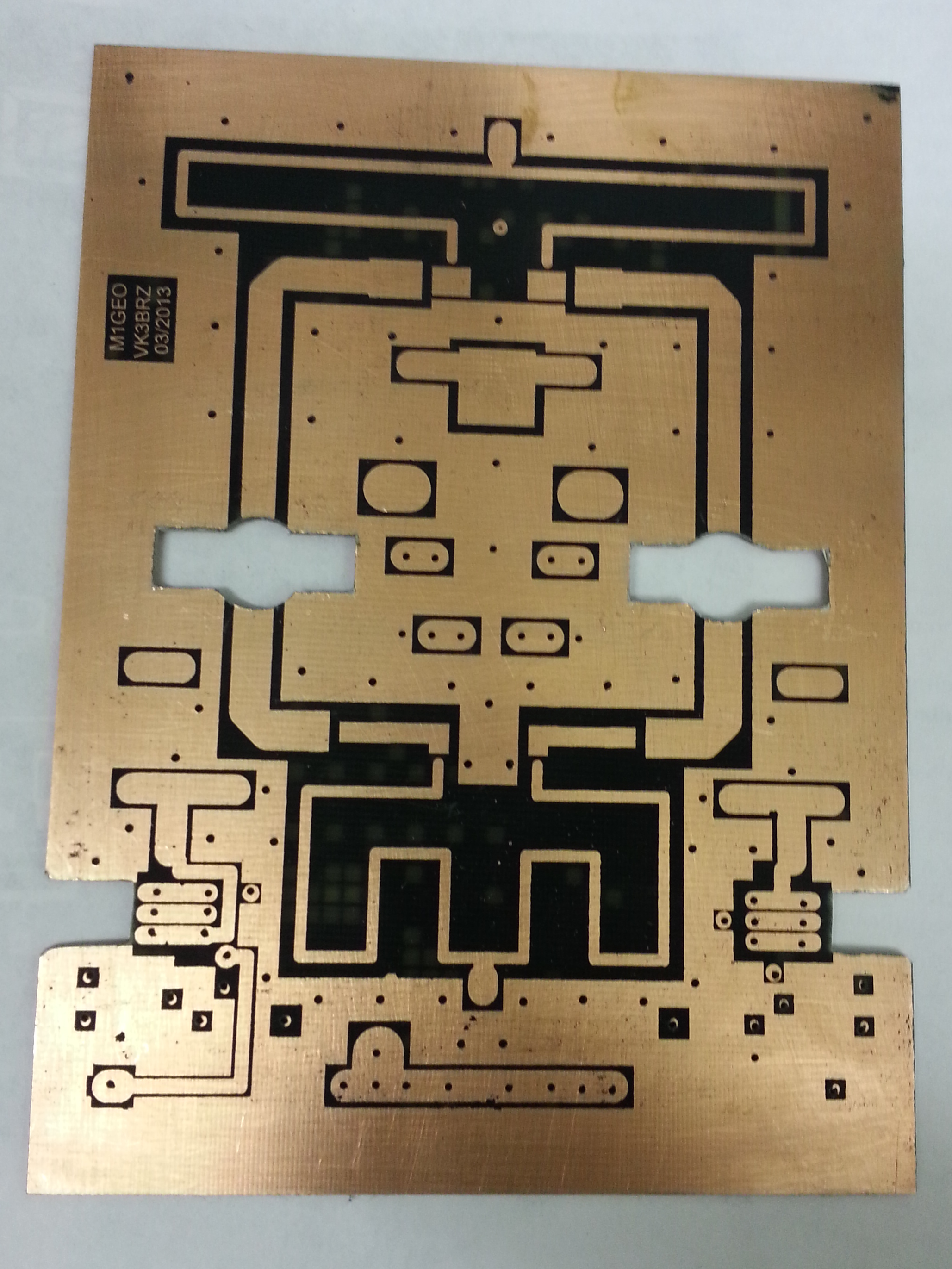
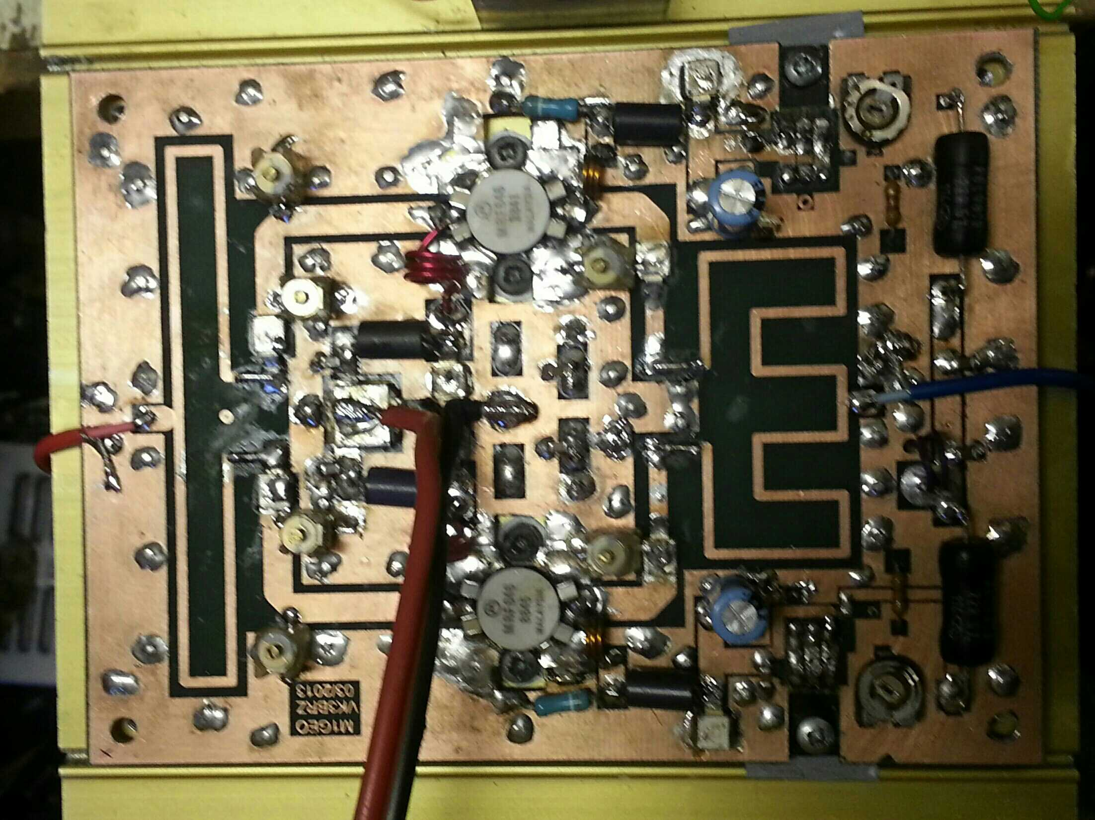
Board Layouts
The following two images are for illustration only. Ensure that both sides of the board match. It sounds silly, but I make this mistake and etched a board where the sides of the board weren’t complimentary. Check with the biasing supply on the bottom of the board. The bump on the bar with the 22R resistors should match on both sides (of course)!
 |
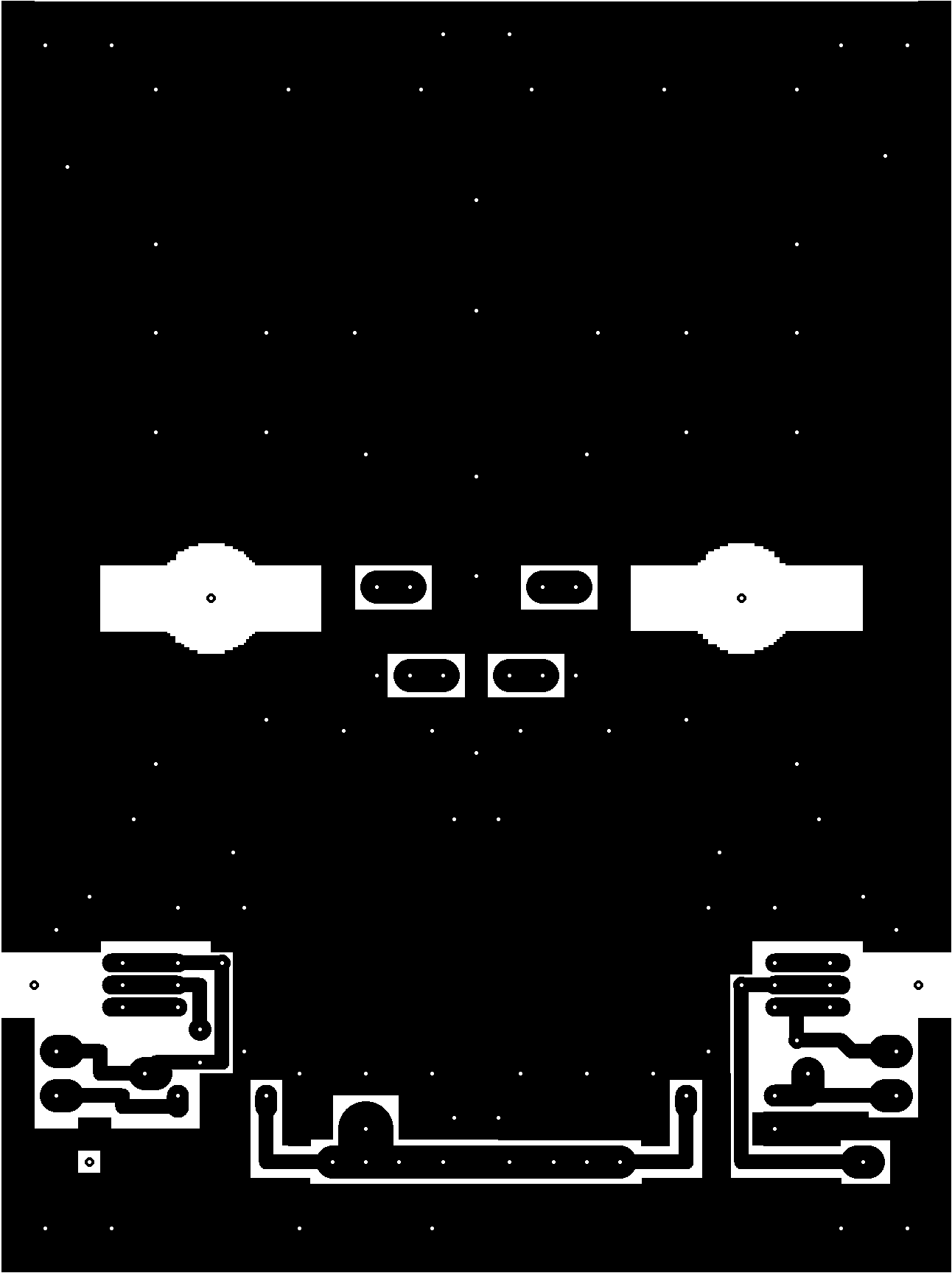 |
- PNG image of both board sides, scaled at 300 DPI.
- PDF of both board sides, print at 100% (unscaled).
- Eagle board layout from IT9VKY’s site, here: uhfpa.zip. I have made some slight modifications from this file.
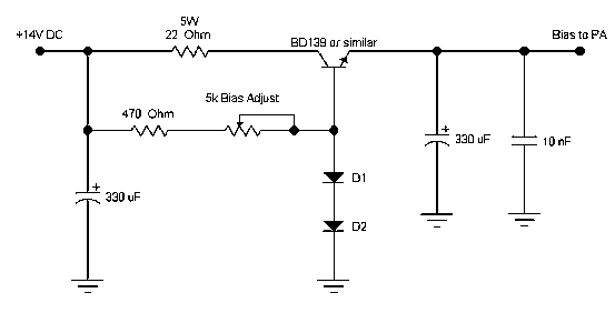
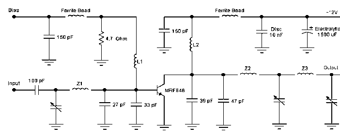
Schematics
These schematics come directly from Eugenio Martinetti (IT9VKY)’s website:
Construction
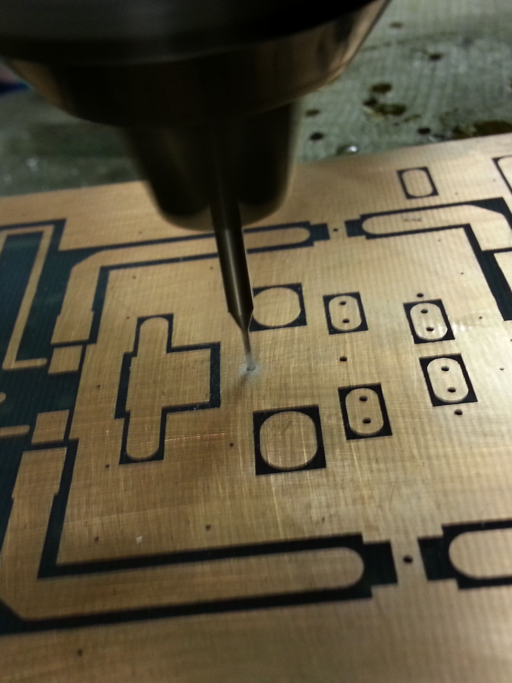
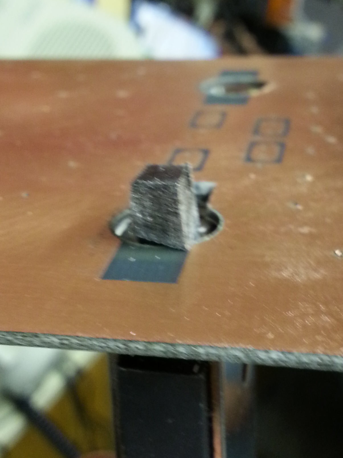
Some image from when I made the double sided board at home:
 |
 |
 |
 |
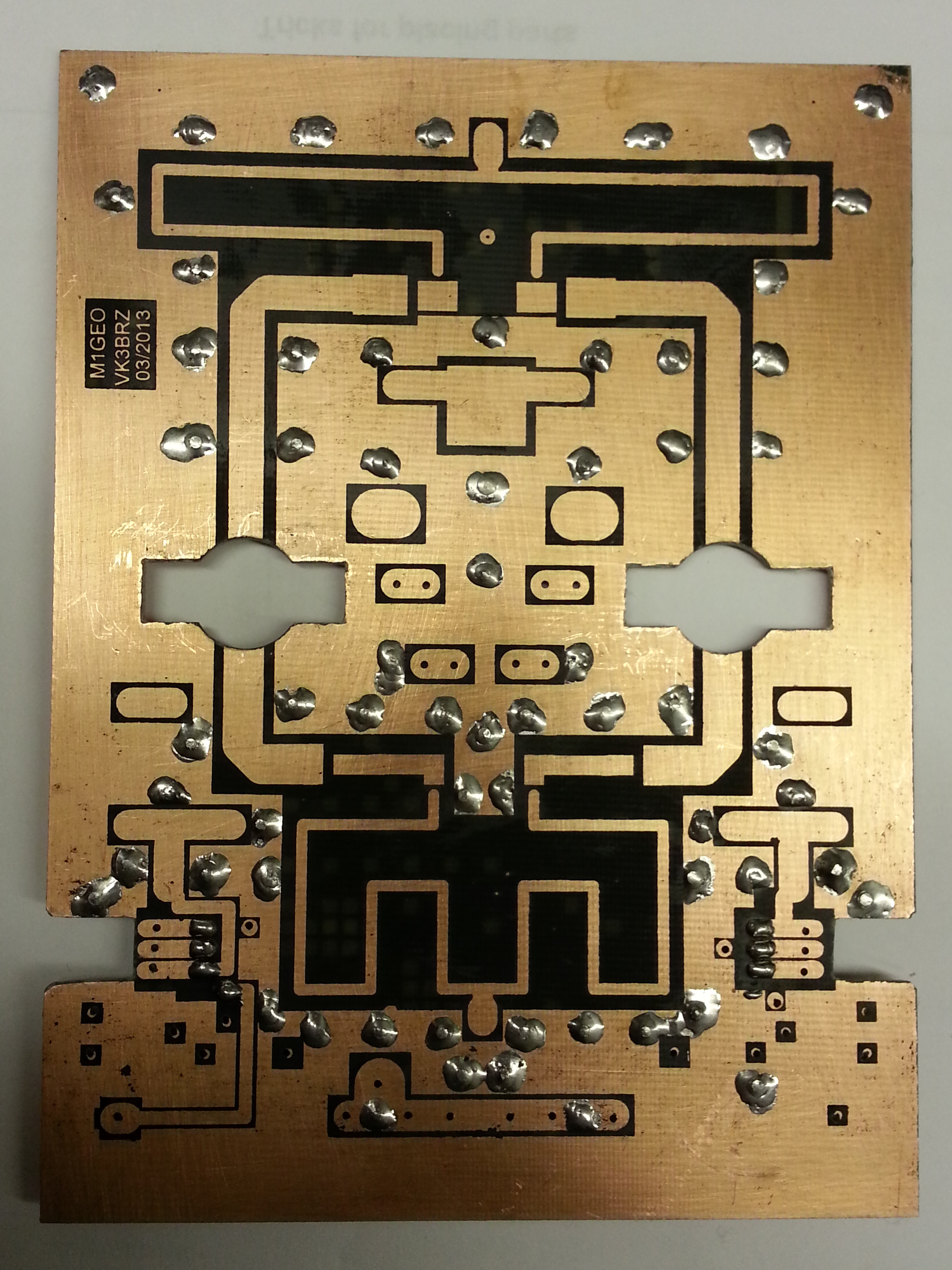 |
I followed Eugenio Martinetti (IT9VKY)’s notes pretty much to the word. My advice is to construct the biasing circuit first off, test that, then process on to the amplifier part. That saves any issues in the bias circuit from blowing the Base-Emitter junction of the MRF646s. At the very least disconnect the inductors to the MRF646 bases. The diodes in the bias circuit are used to track the thermal runaway of the MRF646s. I used two 1N4148 diodes in series as this gave me the closest to 1.2V that the circuit requires. It is quite important to get this right as it’s what stops your transistors from blowing up if they get too hot – that and being careful! They’re mounted in thermal contact with the heatsink. Treat them as if they get hot like the transistors. You want them to!
The initial board I made I had made in work with plate-through holes. These holes were hollow and the plating only very thin. This proved to be a slight problem in the current handling of the board. I added some copper wire through the board around the MRF646s and some tick copper wire on the underside of the board. This greatly improved the current handling and therefore the maximum CW power. Copper film around the transistor emitter flanges is a must, as this helps the current dissipate into the board. The second version of this board I made at home and omitted the plate through holes in favour of drilling the holes and passing wire through. When tested, this method achieved the same higher power output without the added copper wiring.
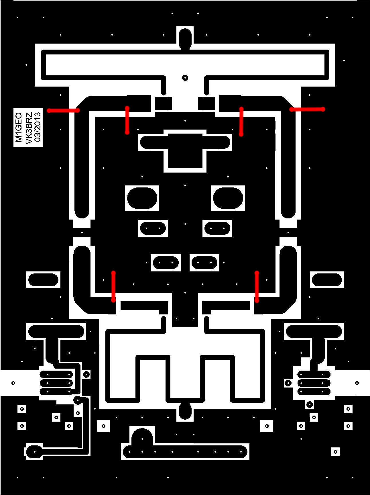
The placement of capacitors on the microstrip lines is important. You have to tap in at the correct impedance. This was something else I found out the hard way. I put them where they fitted best, but it was a mistake which compromised power output considerably. Below the red lines show the placement of the trimmer capacitors. Make sure the screw is connected to the ground side. All trimmers are 9 pF mylar.
The capacitors on the base of the transistor need to go as close to it as possible. As already mentioned, I used salvaged second hand Motorola MRF646 devices. I used ATC ceramic capacitors around the transistors, and metal-clad mica elsewhere but the PMR will have many of the capacitor values you require.
I used two drill bits to give me the correct diameters for the base and collector inductors. I never measured their inductance, simply wound the correct dimensions: 3 turns of 4 mm diameter on the base, 2 turns of 5 mm diameter on the collector. Other pictures show 3 turns on the collector also. I opted for 3 turns on my boards, and they both work well. I can’t say if 2 turns would be better. The ferrite beeds are 3 turns through a 6 hole ferrite.
Adjustment
Don’t do this until you have the board mounted on a heatsink. Even with bias currents, the transistors will get hot and the results are meaningless.
When powering up the amp for the first time, I suggest using a current limited supply. Disconnect the base and collector inductors from the transistor so they have no power supply. Ensure the bias circuit is working correctly and that varying the bias pot adjusts the bias current in the  resistor.
Set the bias pots to their minimum and then reconnect the base and collector inductors to ONE transistor. Now when powering up the circuit, increase the bias pot for a collector current of 100 mA – do this with an ammeter in line with the collector (preferred) or by adding (possibly just over for base current) 100 mA to the current draw with no transistor connected. This puts the transistor into its linear region. Repeat for the second transistor.
At this point your transistors are biased and ready for some RF. Still with only one transistor, apply a signal to the base of the transistor. Note, you cannot put the signal in at the input to the combiner circuit as it uses  matching lines which would destroy the signal integrity before it gets to the amplifier. You also need to remove the two
  balancing resistors. Inject a test signal as shown below – I used 432.2000 MHz at 100 mW from a Marconi signal generator. If you use a radio, keep the power very low at this stage. The red dots show where the input is for each half while the green dots show the grounding points I used.
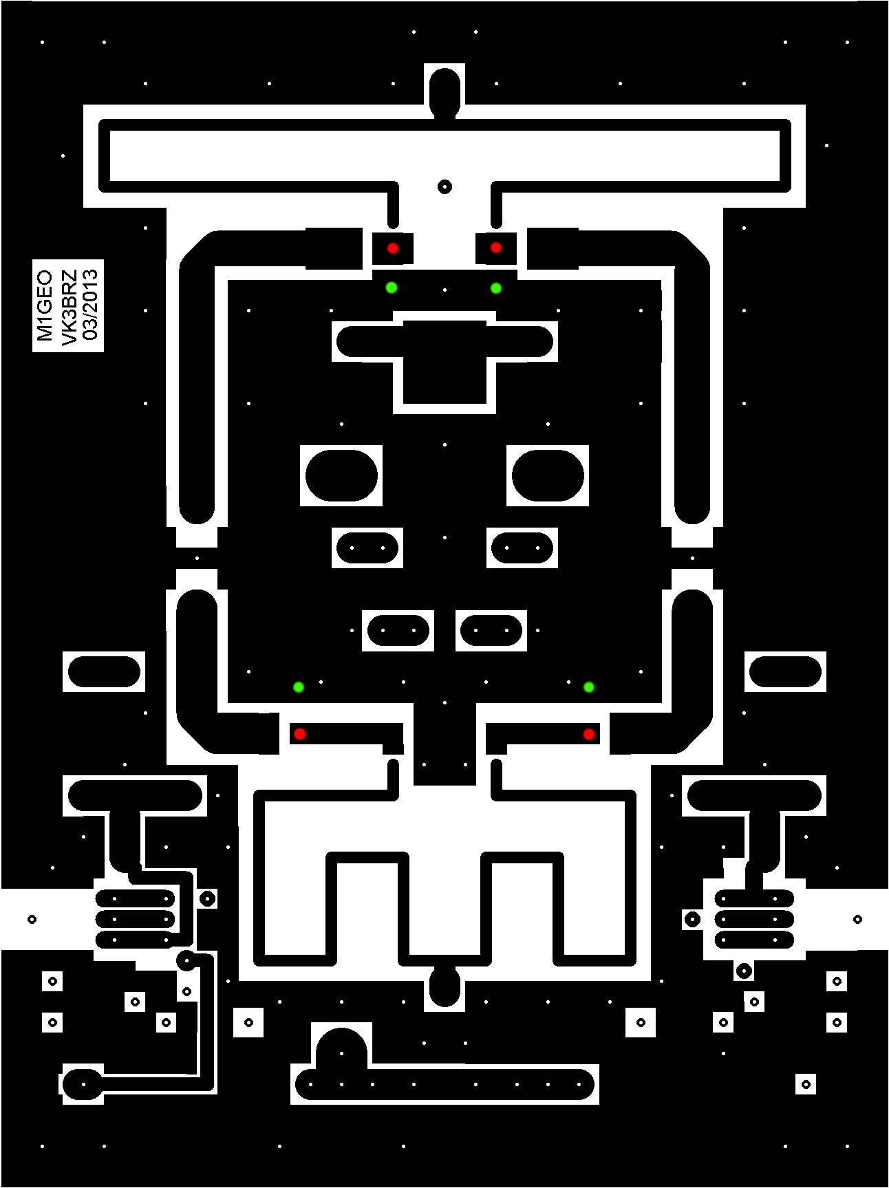
With a power meter and  load connected to the output, apply drive and tune the 3 capacitors for the appropriate transistor. Tune for maximum power (maximum smoke as they say!). The capacitors are interlinked, so you will need to go around a few times until you’re doing okay. There should be again of around 5 times. My 100 mW becomes 492 mW for example. Tune to maximise the RF output on the frequency you want! Then repeat for the other transistor.
Once both halves are tuned, you’re ready to connect the power combiner (blue lines) and add the balance resistors (yellow lines). Move the signal source (red/green dots) to the input of the power combiner and connect both transistor base and collector inductors.
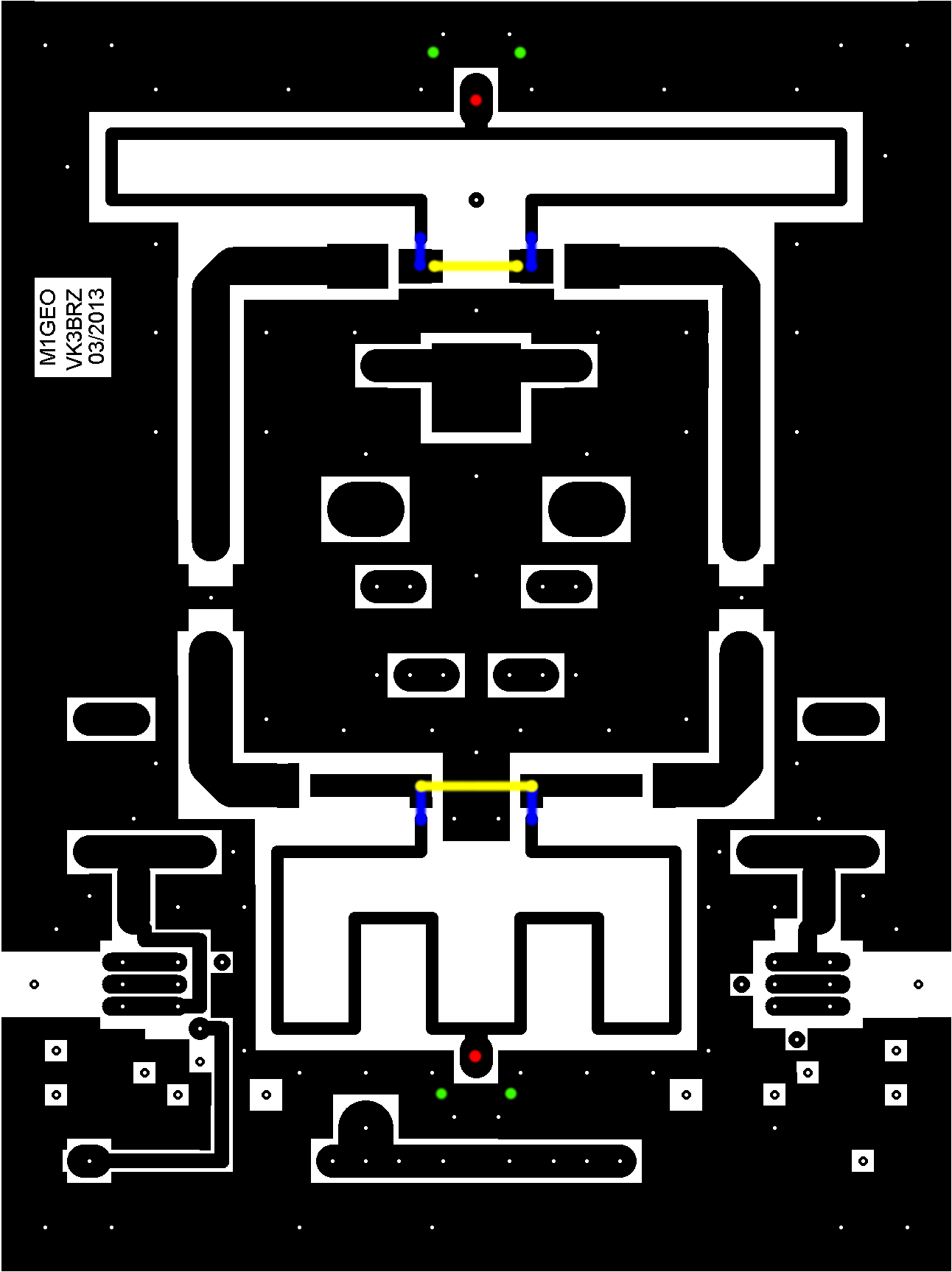
Still at low power, inject your RF into the splitter network. You should still see a gain of approximately 5 times. You will need to re-tune the capacitors slightly at this point – again tune for maximum power at the output on the desired frequency. Now you can increase the drive power to a maximum of 20 W. You should get around 100 W out. At this stage, carefully monitor the transistor temperatures. Any sudden changes in temperature will show up poor thermal conduction to the case which will surely destroy the devices. At a supply of 14 V for 20 W drive I obtain a clean output of 94 W. It may be worth tweaking the tuning at a slightly larger power, say 5 W input (for ~ 25 W output). I would strongly advice against tuning at high powers as mismatches can destroy the MRF646s.
Fingers crossed it will all work. After a fashion, mine did. Sorry the picture is a little out of focus.
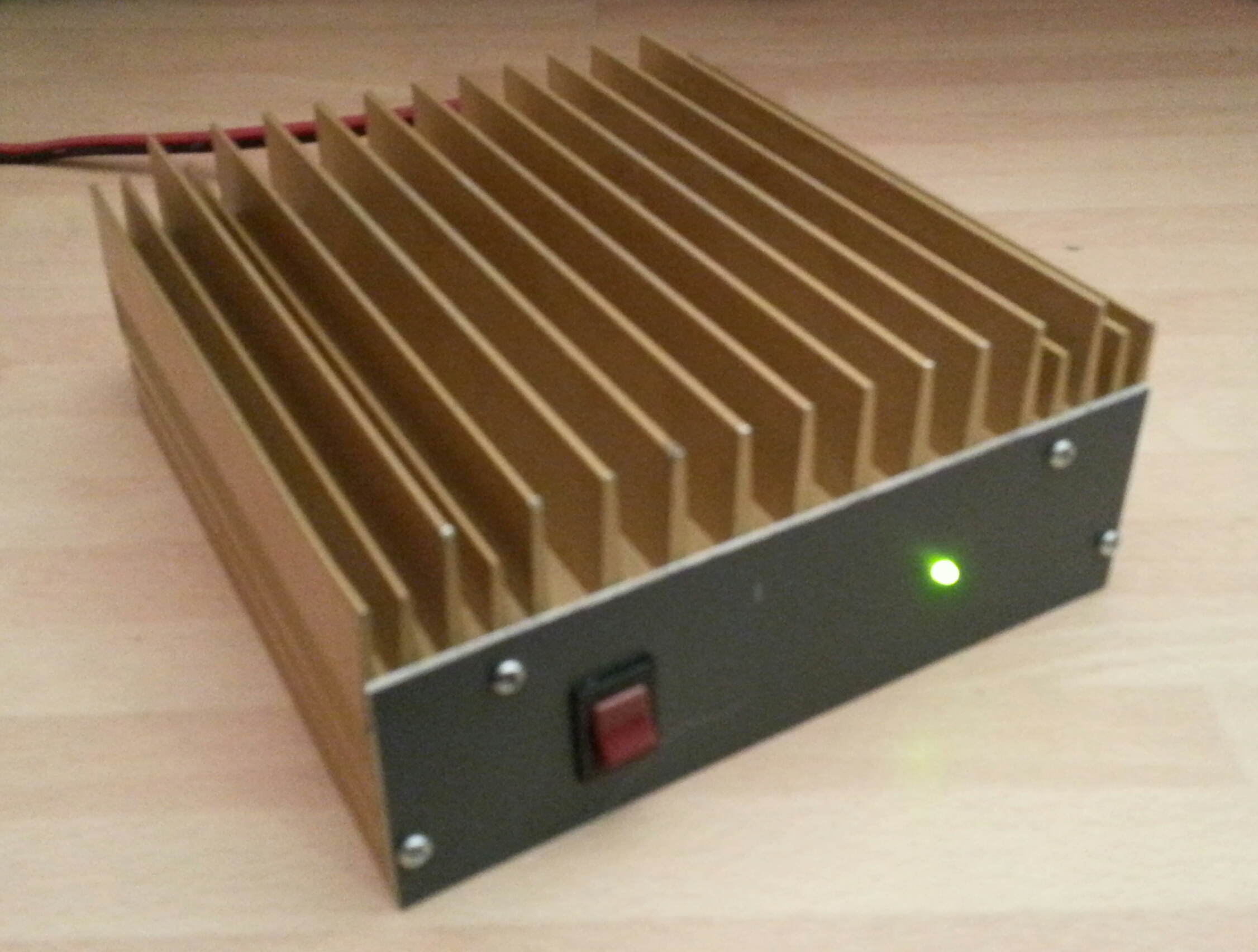
Boxing up
This part of the project is still a work in progress. I used an old Zetagi CB linear amplifier heatsink and remade the front panels using theirs as templates. I used two coax relays as they offered a through-loss of only 0.16 dB (each) as opposed to 4.3 dB for a standard PCB relay. Another PCB relay is used to remove the bias from the transistors when in receive. This removes the linearity of the amplifier, and stops it acting to generate/amplifying noise on receive.
This section is still being written.
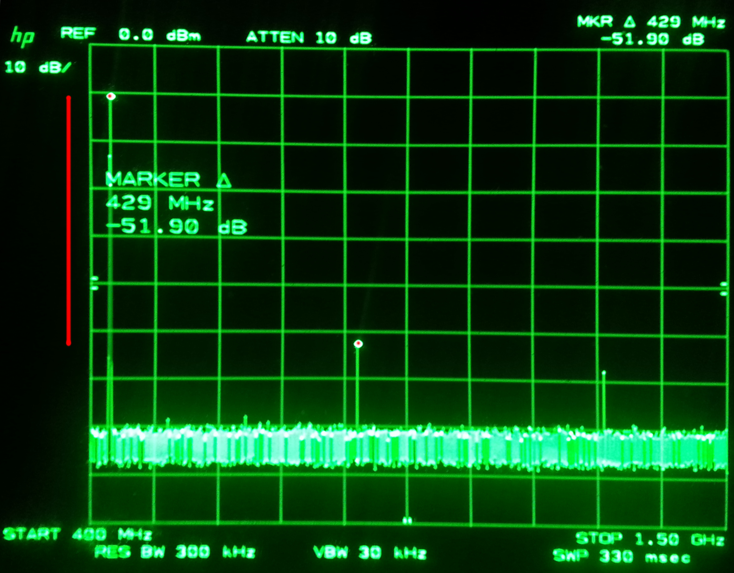
Measurements
Once the amp was deemed to be working okay I wanted to test it on air. I decided that I would measure the harmonic output. Here, I used a HP spectrum analyser to measure the second and third harmonics at the output of the power combiner before the low pass filter. The original article states “the second harmonic is -50 dBc and third harmonic is below -70 dBc. No need for low-pass filters!” Here we see that I achieve similar results for the second but not third harmonics:
 |
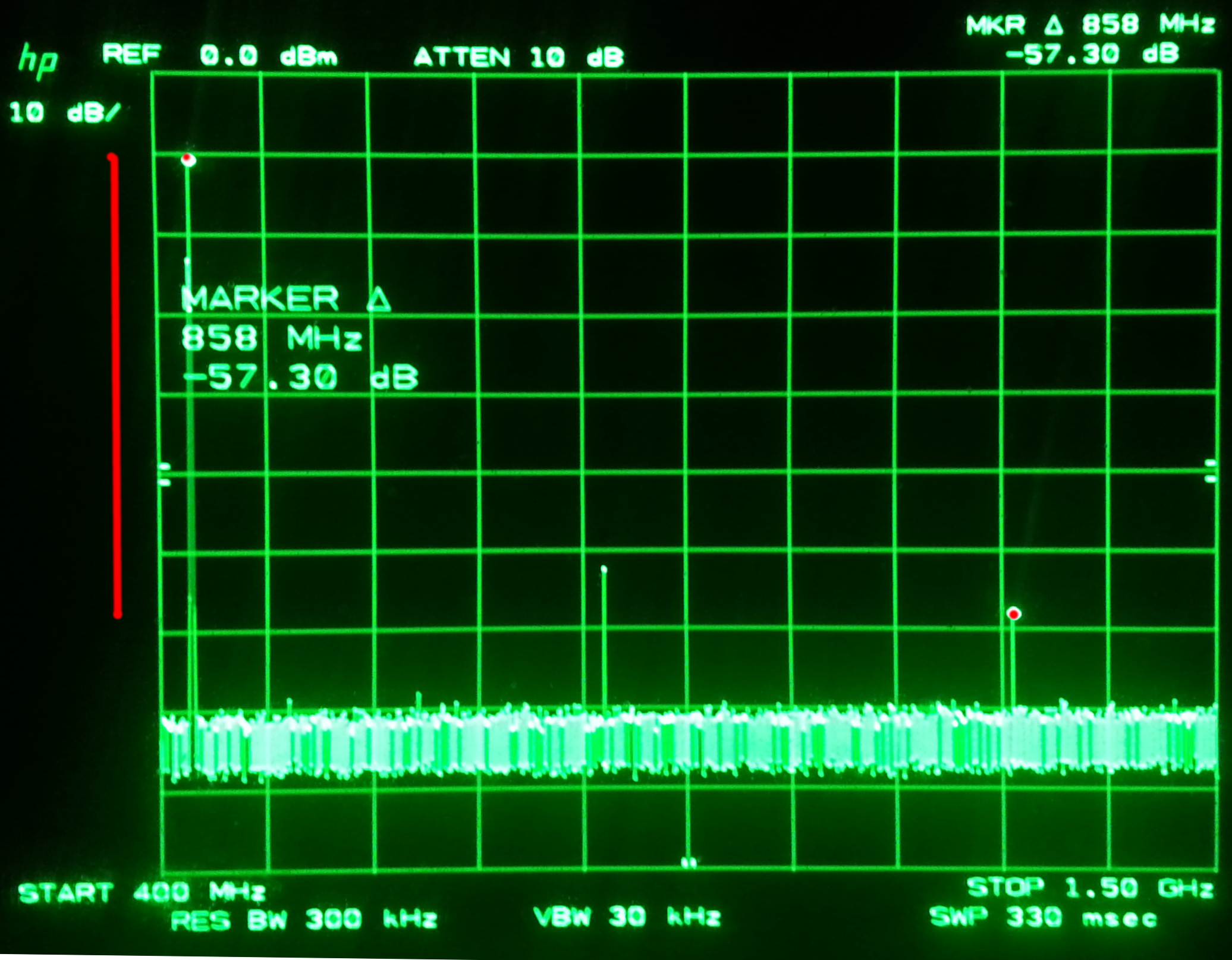 |
Here we see that the second harmonic has a level of – 51.90 dBc and the third harmonic has a level of -57.3 dBc. This was okay for a bit of testing on air, but in the long term, I would like to see at least -60 dBc as is recommended.
The next thing I wanted to check was the linearity of the device…