
This page details how I created a USB DCP (dedicated charge port) in my car for my HTC Desire. This is a permanent installation taking a component level approach. The page also details the testing and compliance with the USB charging standards. If you are looking for something that can be bought of the shelf, this page isn’t for you. However, you may find it interesting.
The Problem
I own a HTC Desire and use it to link to my Car Bluetooth Audio adapter. This allows me to play music and run Google Navigator (a fine piece of software). However, as you can imagine, playing music, running the navigator (which downloads maps via 3G) and the display continuously uses a fair bit of power. Standard USB chargers tend to only offer 500mA at 5V for charging mobile phones via USB. This is the maximum current supplied by a standard USB port. However modern phones require more than this in order to guarantee that the phone will still charge even under heavy battery loads. The HTC Desire’s technical specifications states that 850mA is the maximum current, although in practise (from my own measurements) it has never gone above around 700mA. This page details my investigation into how comes the HTC’s branded charger can keep my phone operational under heavy battery loads but many other third-party chargers cannot.
The Solution
Recent changes within the USB specification make provisions for a USB DCP (dedicated charging port) in which the charger must offer more than 500mA supplied by the standard USB port. The Specification makes clear the acceptable output voltages and currents. I therefore set about making a regulator from the car’s 12V supply (mine can be as high as 14.5V with the engine running).
I had various attempts with switch-mode regulators before settling on a linear regulator for the final design. Although very efficient, switching regulators created switching noise that I just couldn’t eliminate to my satisfaction – this wasn’t so important when listening to music, as the music-to-switching-noise level was very high, but, during a phone call where there are often periods of quiet, this noise was prevalent. The linear regulator, by nature, does not produce any switching noise but is much less efficient – the extra voltage is simply dissipated as heat – and when there is a large voltage difference at a reasonable current, this is a lot of power! Some rough calculations proved this idea to be workable, and so I went ahead and built the final (linear) regulator presented here.
The Design
The design uses National Semiconductor‘s LM 7805 (now discontinued, replaced with LM 75M05). If you are not worried by switching noise (or have more of an idea how to filter it), the LMZ 12010 looks to be a splendid chip with 10A output @ ~92% efficient.
Calculations
The LM 7805C chips I used have a maximum output current of 1.5A. Slightly higher currents result in fold-back current limiting (the output voltage drops to keep current constant). Here is the specification for what I would like:
- Maximum observed supply voltage, 14.5 volts.
- Maximum required current output, 2 amps.
- Over-rated current output, 4 amps. (I wanted to be able to plug two devices in, though this was not required long term. It also ensures the device is over specified.)
Firstly, I calculated how many devices I would require to supply 4 amps.
:
:
: devices
Next, we calculate the power dissipation for each individual device:
:
:
:
:
:
:
:
: (absolute maximum)
Total power dissipation (for all 3 devices) is also calculated:
:
:
:
: (for all devices, at highest voltage & current)
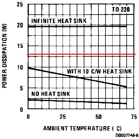
From the inset graph (right) we see that a heat-sink with a thermal resistance of 10°C/W (10°C/W means the heat sink (and therefore the regulators) will be 10°C hotter than the surrounding air for every 1W of heat it is dissipating) allows us to dissipate more power in the device. The heat-sink I have chosen to use (an old CPU heat-sink, bolted to a metal box containing the devices) offers a much lower thermal resistance, and combined with the metal of the car, we can assume the heat-sink resistance close to infinite case on the graph.
Some power will also be dissipated by the balancing resistors ( ). These resistors are used to drop the voltage from one regulator under high currents to account for manufacturing tolerances, i.e. so that one single device doesn’t try to produce the full 4 amps.
:
:
:
:
:
: per resistor
: for all 3 resistors
Combining the resistors power output with the devices as calculated above, we get the following:
: total from system
It’s going to get hot under extreme circumstances, if proper heat-sinking isn’t installed – A good case for switch-mode power supplies if there ever was one! More typical input voltages of 13.8V and one device at 5V, 2A yields a result of  .
.
Calculating efficiency for the sake of comparison:
:
A shockingly low value compared to the quoted 92% for LMZ 12010. The price paid for no switching noise!
The Schematic
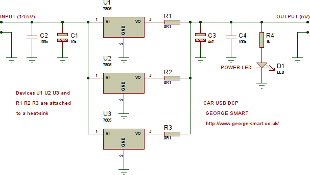
The schematic above is fairly simple. Note that devices U1, U2 and U3 as well as resistors R1, R2 and R3 are bolted to the heat-sink as discussed in the power calculations above. Capacitors C1, C2, C3 and C4 act to smooth the supply removing any noise from it that may be present on the input (i.e. alternator whine, etc). R4 and D1 provide an indication that the device is powered on. This may be removed if you don’t require it.
The output of this regulator stage needs to be connected to a USB-A Socket. The kind found on a computer’s backplate. Two of the wires will take the 5V and ground from the regulator, the other (inner) two, D+ and D- data lines, are shorted together to identify the port as a dedicated charger port. This is shown in the image below. However, my schematic software (LabCentre Electronic’s Proteus Professional) doesn’t have a schematic device for a USB socket, only the plug. So that’s what is here.
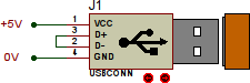
Just to reiterate, your device will need the regulated 5V connected to the socket, and the data lines shorted together to indicate a DCP.
The Made Regulator
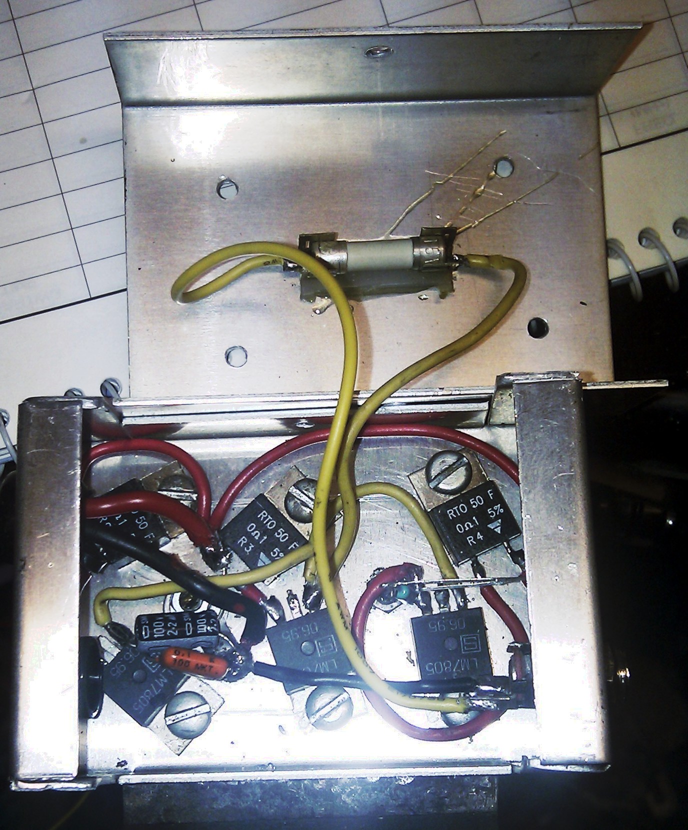
The construction method is clearly not great, but it works fine. I included a few connectors to allow me to disconnect this box and work on it without having to remove and re-run cables inside the vehicle. I run cables from the engine compartment where the regulator is located, to the back of the dashboard and up inside the dashboard storage box (for CDs etc). This then provides a USB port that is easily accessable on the dashboard for powering my HTC Desire or TomTom SatNav (or any other USB Device).
The regulator I built varies very slightly from the schematic.
Testing
My main concern (aside from blowing the phone up) was that the phone wouldn’t treat this as a dedicated charging port, rather using it as a standard charging port. The electrical difference between the two, as mentioned above, is that the two data pins (D+ & D-) are shorted together. However, some places on the internet mention that some mobile phones test the supply, to assess it’s capability of supplying higher charge currents. I decided that if my device complied with the USB Specifications, specifically the Battery Charging v1.2 Spec and Adopters Agreement then that was about all I could do. So I set about testing. The main test for the charger is the load test – a plot of charger terminal voltage against charge current. Section 4.4.1 on page 39 of the Battery Charging Specification, Revision 1.2, December 7, 2010 gives an example graph showing acceptable performances by various charger types so I figured I would plot my charger’s performance onto the same graph and hope that it performs at it should.
The test saw me using a high current power supply (30A) at 14.5V to simulate that of a vehicle. Then, using an artificial load (a device that draws current in a controlled way) the charge current was gradually increased and record made of the charger’s terminal voltage. These valves were then plotted as X-Y scatter points and a line added to ease the eye.
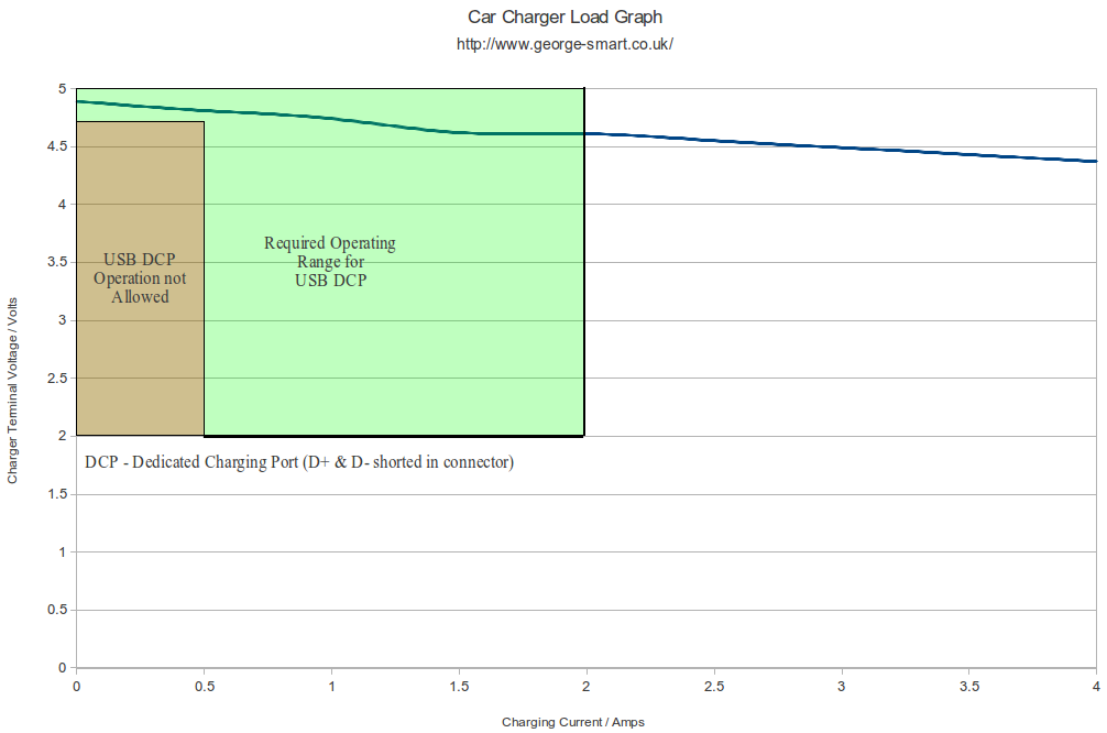
The specification states simply that the load line must provide 2 amps at a voltage greater than 2 volts, and therefore cross at right edge of the green box. For devices that cannot supply 2 amps, they should reduce the terminal voltage such that the load line leaves the green box through the bottom of the green box. The load line should never go inside the red box (if it does, it would be classed as a standard USB port). Here we see that the load line (in blue) meets these specifications exactly.
Conclusion
Some brief experimentation with my HTC Desire reveals that the phone never draws more than 800mA. This is confirmed is various places online. The device I built complies fully with the specification for a USB DCP. Foldback current limit starts at 4.5A and is almost fully shut-down at 5A. This is a feature of the LM 7805. When using my Desire with Bluetooth and Google Navigator, the device is able to keep up charging where as before the device would gradually discharge.
Others note that by supplying 5.5V to the device, the Desire enters the quick-charge algorithm (essentially treating the port as if it is configured as a DCP). However, 5.5V is outside of the specified USB bus voltage, which is an absolute maximum of 5.25V. I opted against this method as it would make the socket in my car non-standard (and possibly lethal to some devices)!
Other than that, the regulator runs pretty cool with just the standard CPU heat-sink to cool it. It turned out exactly as I had hoped.