
Back in November 2019, I was browsing eBay for interesting electronics trinkets and modules, when I saw an advert for a set of 6 new old-stock Russian numitron tubes. I paid around £16 for the 6 tubes, but the price appears to have increased a little in the interim.
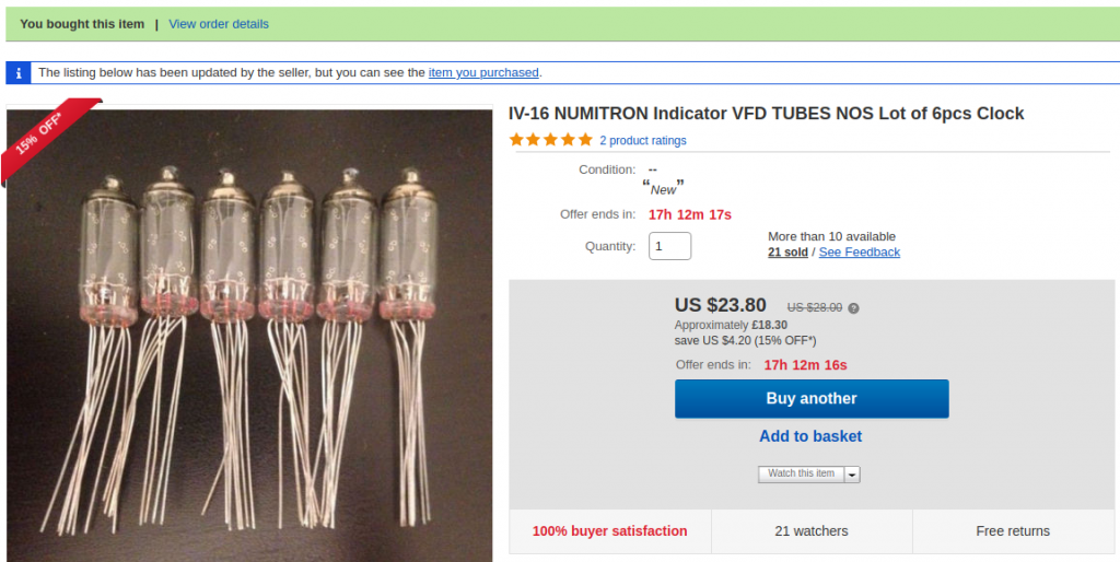
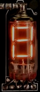
These numitron tubes are often confused with nixie tubes, both with an orange glow. However, the principles of operation are very different. People are more commonly familiar with the nixie tubes (or nixies) which operate at high voltages (typically ~180V DC) with each numerical digit created from a piece of metal inside a glass envelope filled with neon gas. When the voltage is applied, the electric field causes a glow around the negative cathode terminal (shaped like a number). In contrast, numitron tubes use incandescent filaments set out in a 7-segment style arrangement to create numbers.
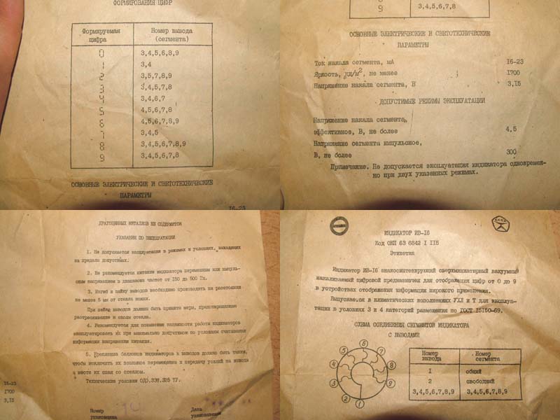
The first thing to do was to learn how I would need to drive the tubes. Since they are incandescent tubes, I figured they’d need a reasonable amount of current to illuminate the segments, but I wasn’t sure at which voltage. Fortunately, I was able to find a datasheet which suggested a filament voltage of up to 4.5V. The Tube Store website has some detailed information on these tubes.
Using this information, I had started developing a plan in my head. I knew that a small MCU could be run at 3.3V and would drive 25mA from an IO pin, so I decided to see what the tube looked like at 3.3V. Using a lab power supply I could see that each filament was drawing around 18mA – importantly below the 25mA IO limit! This was the deciding factor, since this means that there is minimum interface logic: no voltage level conversion on current limiting.
After a little more thought, I wondered if I could create a minimal design – I wondered if I could create a one-chip-wonder!? If I used an MCU such as an Arduino or PIC as I have done in the past, I would need some kind of external drive circuitry. If I used an FPGA, I would have enough IO pins to drive every segment directly with no extra logic, and the FPGA could (caveats here) drive all of the pins directly with no interface at all; literally coming from the FPGA IO, through the filament to ground.
After a few back of the envelope calculations, it became apparently that doing so would be pushing the FPGA’s IO banks quite hard. I settled on a Lattice LCMXO2-640HC-4TG100C. The Lattice parts are quite simple to use and are a good price – this part cost me £4.58 from Mouser and has 78 IO pins available. I would need around 50 IO pins; 42 (7 segments x 6 digits), 4 (colons) and 4 (buttons). I also provisioned for a set of DIP switches to set an alarm and a loud speaker. In the end, these never made it on to the PCB as I had wanted to keep the project small. The FPGA IOs are rated to 25mA, but there is a limit to the IO bank dissipation which this project does exceed. To (slightly) help with this, I configured the project to have the FPGA sink current instead of source it (less internal resistance in the IO banks, thus less on-chip power dissipation). This is poor practice, but, I was striving for a one-chip solution.
The board needed a power supply, and I opted for micro-USB. I chose the AZ1117E-3V3 (1A) LDO regulator as the 5V to 3.3V because I wanted to keep things simple – in hindsight, I should have used a switching supply, as this regulator gets quite warm.
The ECS-327TXO-33-TR 32.768kHz oscillator was used to keep time. You can basically use any frequency, since there’s plenty of FPGA fabric to create any divider circuit you need to obtain a 1Hz clock. 32.768 kHz (or MHz) are common, since they divide easily by a power of 2 (2^15) with simple counters.
The colon digits that flash with the new second ended up being small model railway bulbs. I went through several parts before settling on 5V ‘grain of wheat’ bulbs; these gave just enough glow at the lower 3.3V supply, without drawing huge amounts of current. Each bulb is individually driven, allowing for more sophisticated display patterns.
All that remained was a header to connect the programmer and a few test LEDs: power, 1 PPS and “DONE” (which shows the FPGA programmed OK/debug LED).
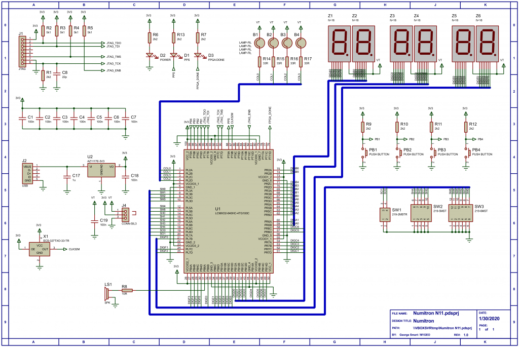
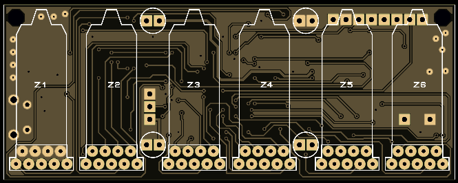
Using the datasheet and a set of vernier calipers, I was able to create a simple PCB footprint. I decided to have the tubes mount with their backs flush to the PCB, not standing up. The board design was lazily done. I positioned the FPGA in the middle, orientated most appropriately (in hindsight, this should have been rotated 45°), the tubes and buttons, USB connector and other hardware components. I routed around the filaments by hand, and then used the auto-router to fill in the missing traces, carefully specifying the design rules, etc.
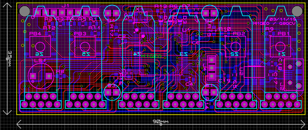
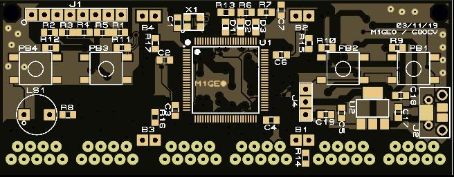
Overall, I was very happy with how the project turned out. The first batch of boards had a small issue where one segment of the LCD was not correctly connected – this was due to the pin-out showing the bottom of the tube, not the corresponding pad layout for the PCB. This was due to my inability to read Russian. A Russian speaking colleague uncovered my mistake! In the video at the top of the page, you can see 6 short ‘bodge wires’ on the back of the board, behind the tube solder connections.
The hardware on the board was about as minimal as I could make it. The there are only 3 ‘active’ components on the board – 6 if you count the debug LEDs which are optional:
- FPGA
- 32.768 kHz oscillator
- 3.3V regulator
- debug LEDs (x3)
The Verilog in the FPGA is pretty simple, and publicly available. It is largely my own work, but takes influence from other sources – these are indicated in the source files concerned. The files make up a complete Lattice Diamond project. You can download/view the files on GitHub: https://github.com/m1geo/IV16-Numitron-Clock.
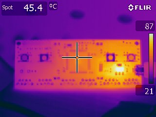
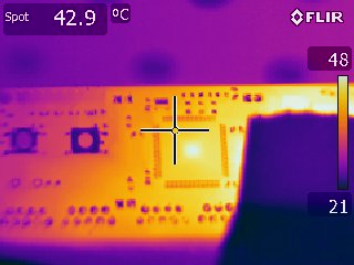
The clock has been running for around 2 months at this point and has never missed a beat. A quick look at the FPGA package with a thermal imaging camera shows the package to be warm, but not ridiculously hot. The whole project runs warm because of the filaments – after all, it’s wire glowing red hot! From the thermal images of the worse case (all segments statically on) that the voltage regulator gets pretty warm – around 87°C. In this circumstance, the regulator is dissipating around 1.4W with little (realistically no) heat-sinking. Meanwhile, the FPGA package is around 45°C.
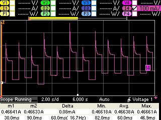
The project draws around 700mA with all segments illuminated. A more typical current draw is around 500mA, but this clearly fluctuates throughout the day and throughout the hour, depending on how many segments of the display are illuminated. The characteristic spike and decay is caused by cold filaments (primarily the colons) drawing high current until they begin to get hot, and then tailing off as they reach temperature plateau.