The final STL files can be found at Thingiverse 7267147 – A 30m loading coil for the MC-750 or MA-12 antenna — scroll to the Final Build section for a TLDR.
Background
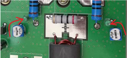
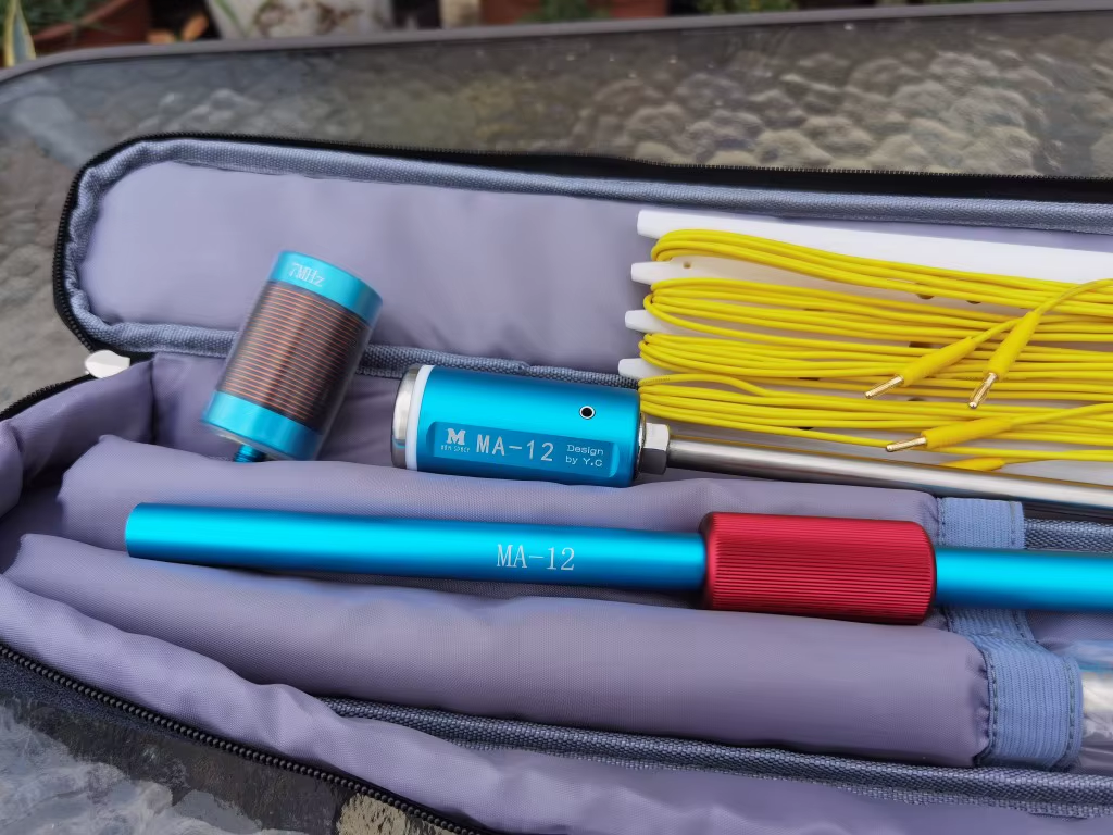
With my interest in SOTA and POTA I have been using an MA-12 vertical antenna for activating since it is convenient and quick to get on air. It seems identical to the MC-750 by Chelegance, but half the price!
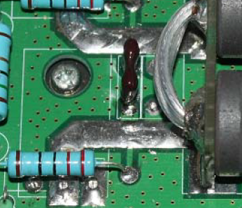
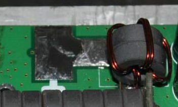
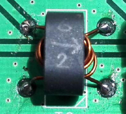
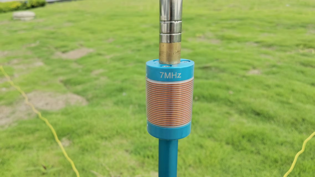
I really like the antenna and it performs well since on the higher bands it is an unloaded vertical. On the lower bands, the antenna comes with loading coils for 40m (7 MHz) [supplied] and 80m (3.5 MHz) [optional]. These are fixed coils, made from copper wire, and so avoid the higher resistances seen on coils made using stainless steel like that of the JPC-7 antenna which uses a variable inductor.
Combined with my learning CW, I have an interest in the 30 metre (10 MHz) amateur band which the the MA-12/MC-750 doesn’t cover (it does, but clearly as an afterthought).
On 30m, the operating manual for the antenna says to use the 7 MHz loading coil and reduce the length of the whip down. Doing this you are able to get the antenna to resonate within the 30m band, but it leads to poor efficiency since most of the whip is collapsed and the antenna is significantly shorter than it could be if the loading coil were sized correctly. So why not make a coil for 30m…
Cue this page…
What inductance do we need?
To find the inductance needed I decided to use the aforementioned JPC-7 variable coil in place of the 40m since it can be adjusted – this meant I could iteratively sweep through all the inductor tap points and see where the antenna resonates.
Clearly there are many combinations of coil inductance and whip length that will work, so I settled on having the whip as long as practical. Rather than using the full length of the whip (5.2m), I opted to leave one section collapsed allowing for some room to adjust depending on ground conditions (rocky, wet, dry, etc.). This left me with a whip around 5 metres long.
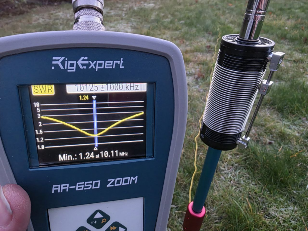
Starting at minimum inductance (top, closest the whip), I could see the antenna’s resonant frequency at around 12 MHz, and as I repeatedly clicked in another turn of inductance on the JPC-7 coil, the resonant frequency dropped.
At 10.8 MHz, I knew I was close, and since an additional turn on the coil took me to 9.9 MHz (below the target of around 10.125 MHz) I went back to the 10.8 MHz tap point, and lengthened the last whip section slightly. With 1/4 of the section extended, the resonance was on 10.11 MHz near enough. The tap was set to 7 (complete) turns.
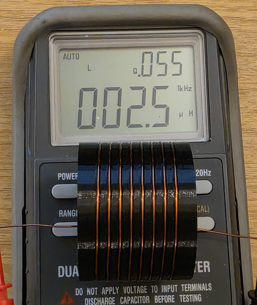
Nice! It was then just a case of measuring the inductance between the two M10 fixings to determine what inductance was needed:
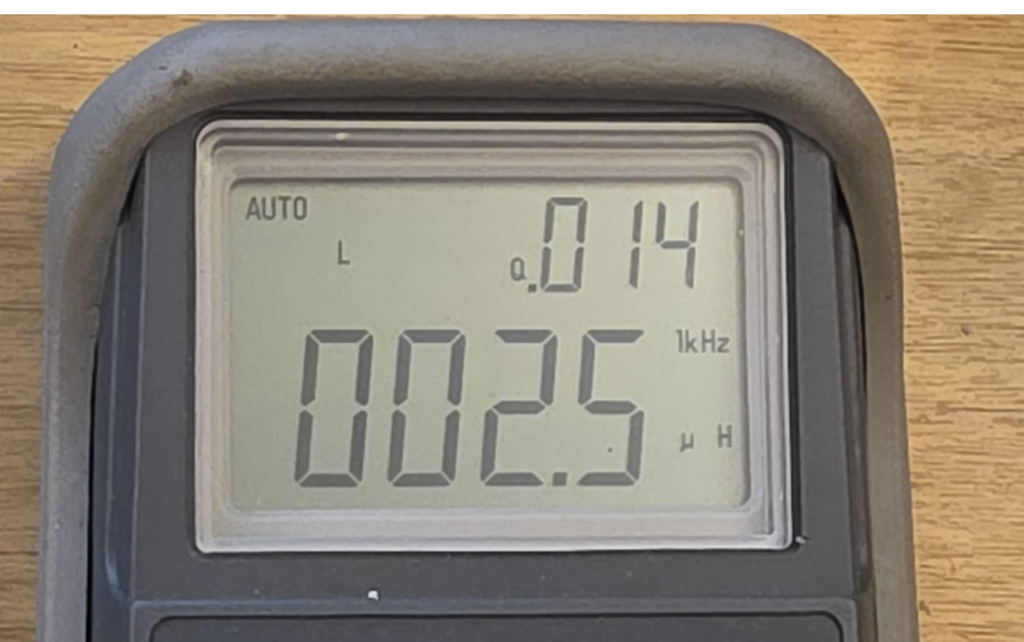
As can be seen from the LCR meter display above, the measured inductance was 2.5 μH after calibrating the test setup.
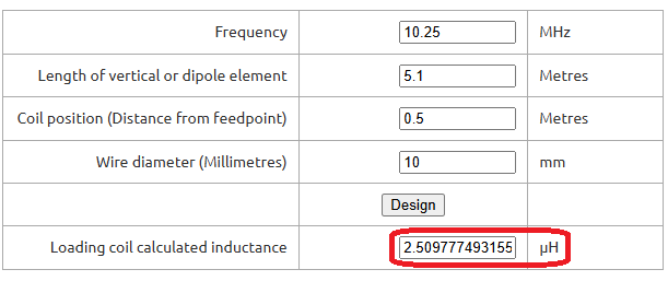
To confirm this was sensible, I put some numbers into John M0UKD’s Loaded Quarter Wave Antenna Inductance Calculator and checked the results. Amazingly, they agreed very well – the calculator predicts 2.51 μH. Wow! I wasn’t expecting that!
For what it’s worth, I run the numbers on the JPC-7 coil, and 7 turns on the 41 mm former over about 10 mm works out about 2.9 μH. Not quite as close, but certainly within measurement errors.
Confident that I had found the right inductance, I then had to make something suitable.
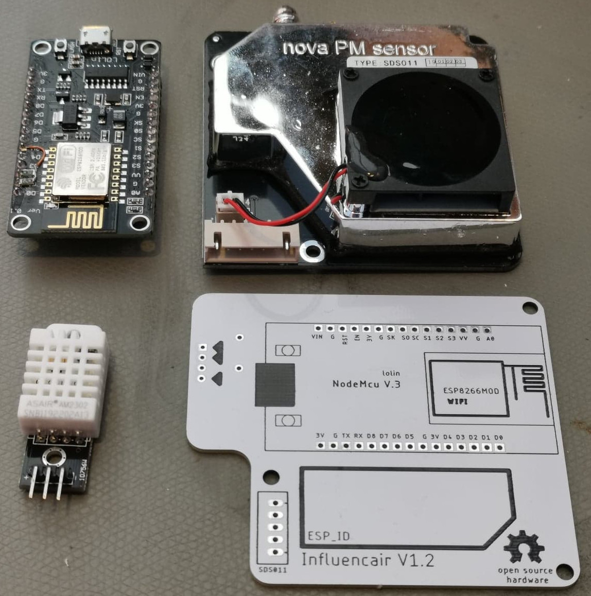
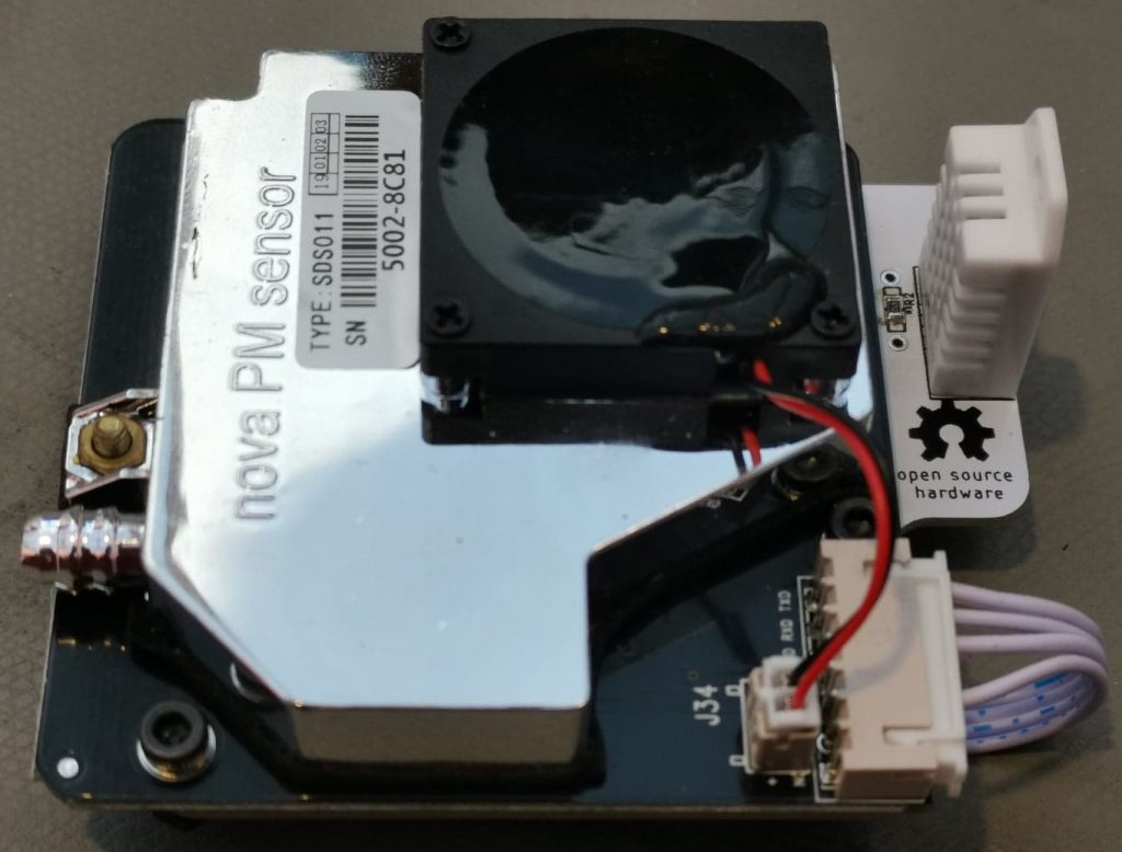
Making an inductor
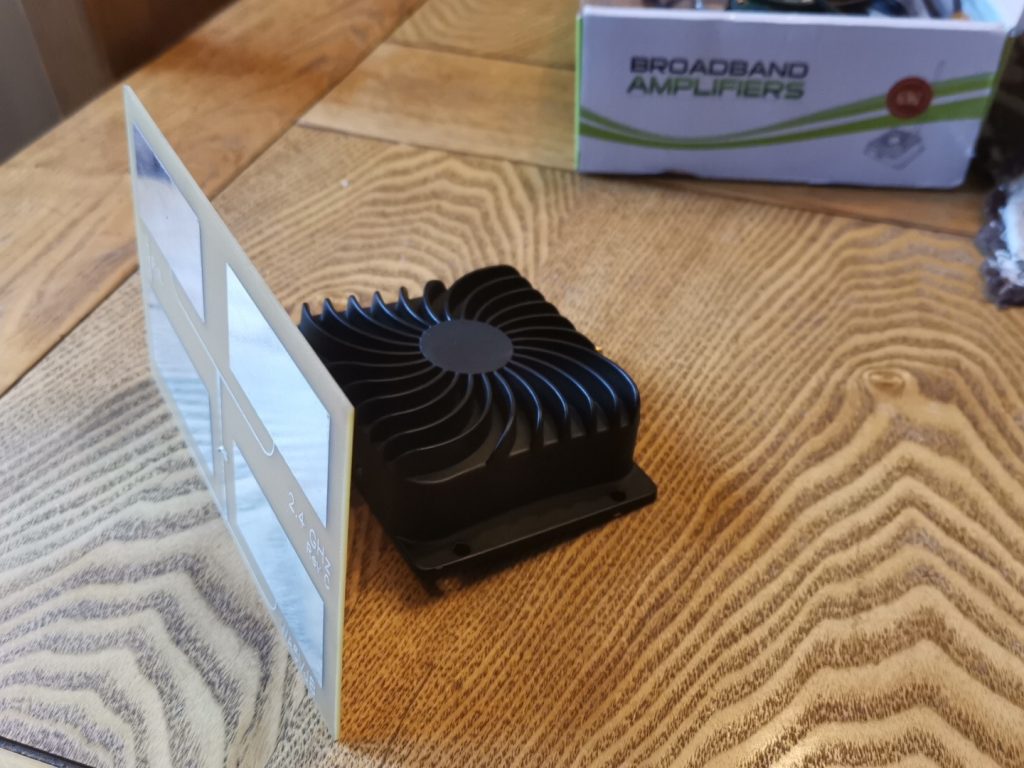
Since I wanted to be able to 3D print the design, a larger diameter coil would be advantageous as it both reduces the length of the coil (and thus leverage from the whip) and increases the glueable surface area (increasing bond strength). Brass M10 nuts and bolts can be purchased cheaply enough in small quantities that it avoided pulling in favours from friends with a lathe, so I chose that route for the connections. Brass can be soldered to, which was the attraction there.
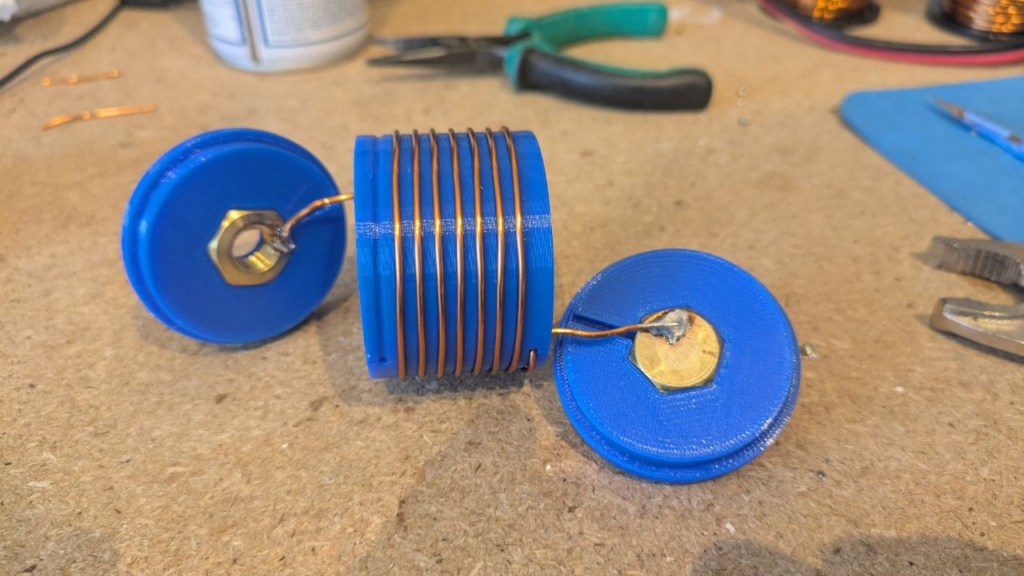
With that in mind, I created the end caps with recesses for holding the nut & bolt tightly. The diameter I chose – based on feel – was 50mm outer diameter, with an inside diameter of 45mm, creating a wall thickness of 2.5mm. A 6mm overlap should provide ample overlap to glue everything up once built. A groove on the inside provides a location for the wire to be trapped under the nut/bolt should the be preferable, though I plan to solder to the fixings. A thin brass washer may also be used.
With the end caps designed, I just needed to work how many turns we would need. This is a bit of a juggling act, since everything about the coil affects everything else – it’s just a case of starting somewhere and tinkering until you get everything in harmony.
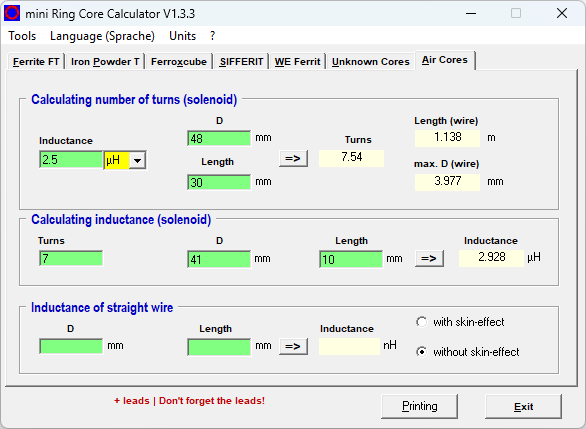
For these projects, mini Ring-Core-Calculator by DL5SWB & DG0KW is the go-to. The calculator has an “Air Cores” mode which fits our needs perfectly. In the top section, you’ll see the desired 2.5 μH inductance, the 48 mm diameter (50 mm minus 1 mm for wire diameter), and the coil length – here I chose 30 mm as it looked about right; the tool tells us we need 7.54 turns.
Note; in the middle box you also see the 7 turns on the JPC-7 coil’s 41 mm diameter former over 10 mm equating to around 2.9 μH. These were just rough measurements taken from the JPC-7 coil used above to further sanity check our numbers.
With those numbers from the tool for our coil in mind, it was time to create the coil former. This is a fairly simple task for someone competent with CAD, but it took me the best part of an hour to get this designed matching what the calculator told us.
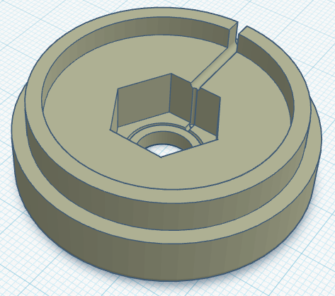
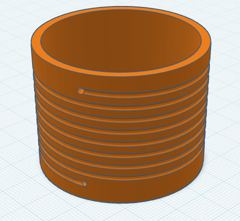
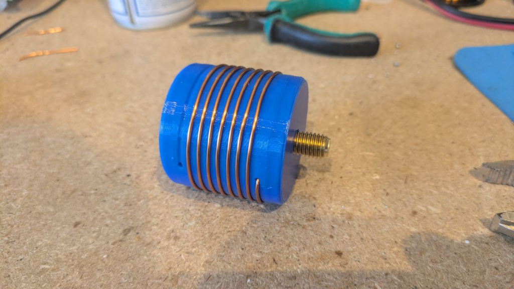
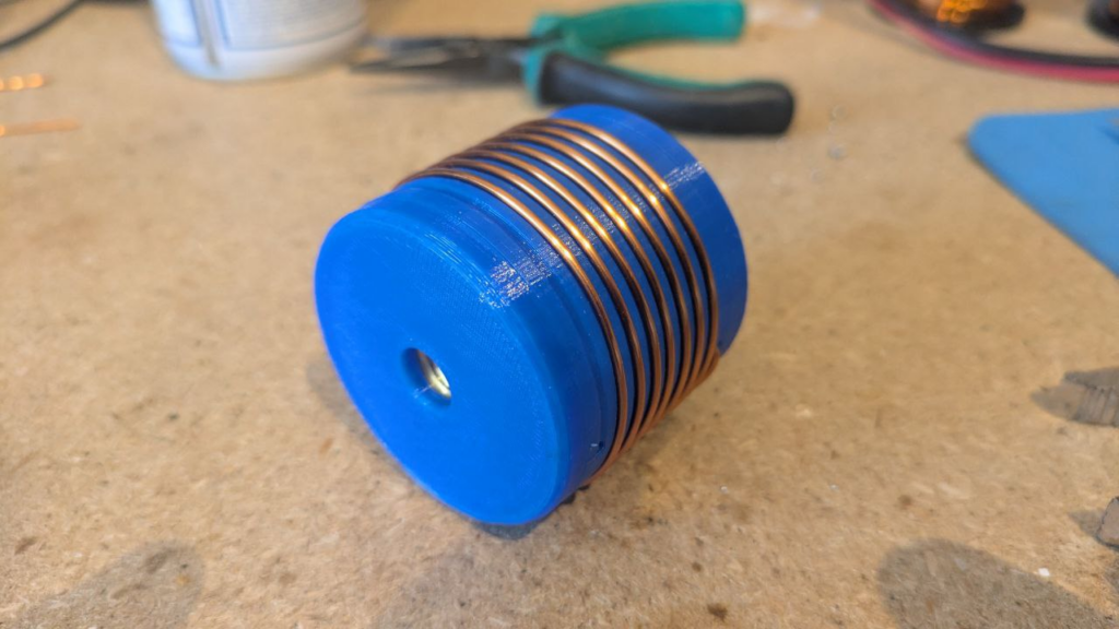
When creating the model for the former, I used 8 turns and then added a hole half a turn back for 7.5 turns too. This allows us the option if needed, but the couple of prototypes I tested showed 7.5 to be the best option (8 turns had 2 sections of whip collapsed in, but also worked fine).
The image below is the 8 turn coil, though latest update shortens it a bit on each end to keep it compact.
Once everything was designed it was time to fire up the 3D printer and get working. If you don’t have your own 3D printer and wish to follow along, many online services like JLC3DP or PCBWay 3D Printing can help – I’ve no affiliation to either, but have used both services more than once with good results – or ask at your local radio club or maker space. Everything will fit on a very standard 3D printer, there’s nothing special here. You may wish to consider the stresses and sheer lines in the print for longevity, but for these parts you see here – the first prototypes – I just printed them as quickly as possible.
Perhaps use a higher infill on the end parts, as they may see leverage from the whip on quite a small area under the nut. I’d recommend 50% infill under the nut & bolt, and then reduced away from that. Though try it first and reprint if they fail?
I printed my parts in PETG as it’s better in UV light and a bit better at handling heat than PLA, but in reality anything should be fine. 0.2 mm layer height, 0.4 mm nozzle, 20% infill, but as I say, whatever you have will be fine! There’s nothing special here. Printing took around 3h45m, used 42g of PETG, costing approximately 2 USD.
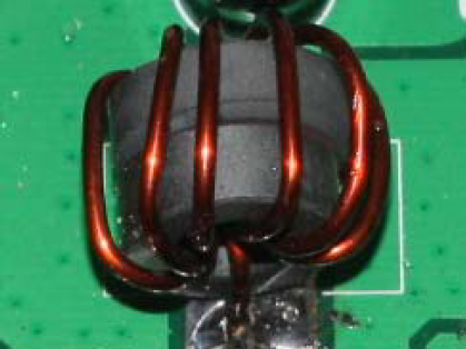
Once your prints are done, you’re ready to wind the coil! 8 turns of copper wire, with the ends finishing inside the coil, since that’s there they’ll connect to the nut and bolt – leave the wires on each end long for now so we can connect things up! The coil calculator tool suggests 1.13 metres of wire is needed for the coil, so I cut 1.2 metres (4 ft) from my reel.
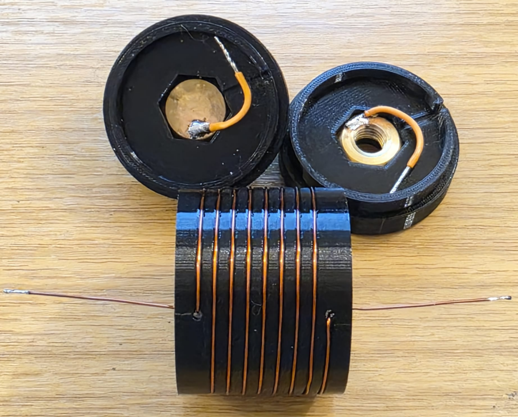
Be careful when soldering not to melt the 3D printed former, especially with heat tracking back up the coil wire through the holes. Solder to the nuts and bolts outside of the plastic. Above I just have some test wires connected, but they’ll be replaced with the proper wire from the ends of the inductor on the real coil.
At this stage, if you can, I’d recommend checking the coil inductance. We’re targeting a 2.5 μH inductance and as you can see below we’ve got that. This meter lacks precision, but we’re at least in the ballpark. Note that the Q-factor is 55, which is a little low on this test coil; I suspect due to using thin (0.6mm diameter) wire. For a 2.5 µH air-wound inductor such as ours, the expected Q-factor typically ranges between 50 and 200 for general-purpose designs and we’re at the very bottom of that range.
An interesting aside, the Q-factor for the stainless steel JPC-7 was very low at just 14 (seen in the image above). Other people have noted this before and Clint KA7OEI has an article on rewinding the JPC-7 using silver coated copper wire to significantly improve its performance but Clint reports seeing Q-factors as low as 11 on the original coil on the 20 meter band and slightly better at the higher inductances needed for 80 meters, with Q-factors of around 30. These values increased significantly to around 60 with standard copper wire and up to around 150 with thick silver coated wire; so once again we’re on the right track given the thin wire I’m testing here. I haven’t got anything suitable to hand but I have ordered some standard 1mm diameter copper wire.
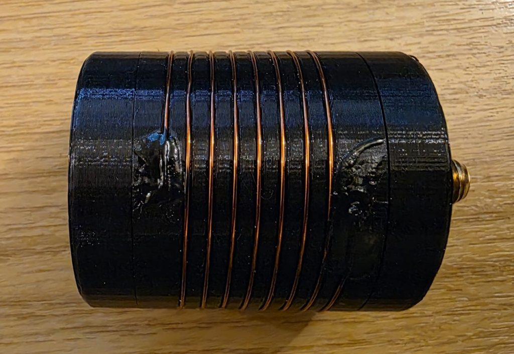
Now lets bundle it up into a coil and see if it works! I used a combination of glues to hold the wire into the coil former; superglue on the wire, holding it into the hole; liquid electrical tape atop, to protect the superglue and help with weathering. Each was allowed to set fully before applying the next. I then made the connections to the nuts and bolts, ensuring the wire did not coil up inside the first. Keep connections at right-angles to the coil, and avoid loops. From the outside, mine looked like this.
Testing
Once the prototype was ready, it was back out into the (cold, −3C) garden to test things out.
[[VSWR PLOT HERE]]
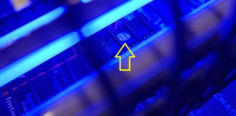
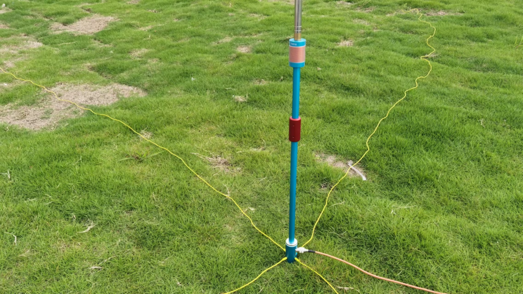
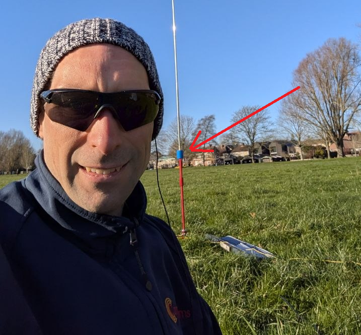
With the VSWR plot looking OK, I managed to convince Rob M0VFC to come out portable with me to Stourbridge Common Local Nature Reserve in Cambridge to activate POTA GB-5467. Rob took on the task of trying the coil out on 30m, and had it up and running in no time, having easily found resonance using the Elecraft KX2 built in SWR meter. Rob took a selfie while I was operating and you can see the coil on the antenna encased in blue heat-shrink to help hold things together.
Final build
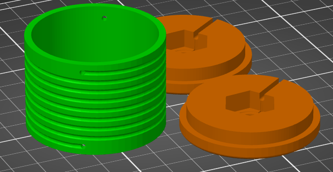
The final STL files can be found at Thingiverse 7267147 – A 30m loading coil for the MC-750 or MA-12 antenna. You’ll need to print two end caps, and one loading coil centre.
After a couple of POTA activations with the coil, it turns out that 7.5 turns allows for slightly more whip expanded, and therefore theoretically fractionally better performance. Below, Rob M0VFC’s build of the coil with 7.5 turns, showing the internal assembly steps.
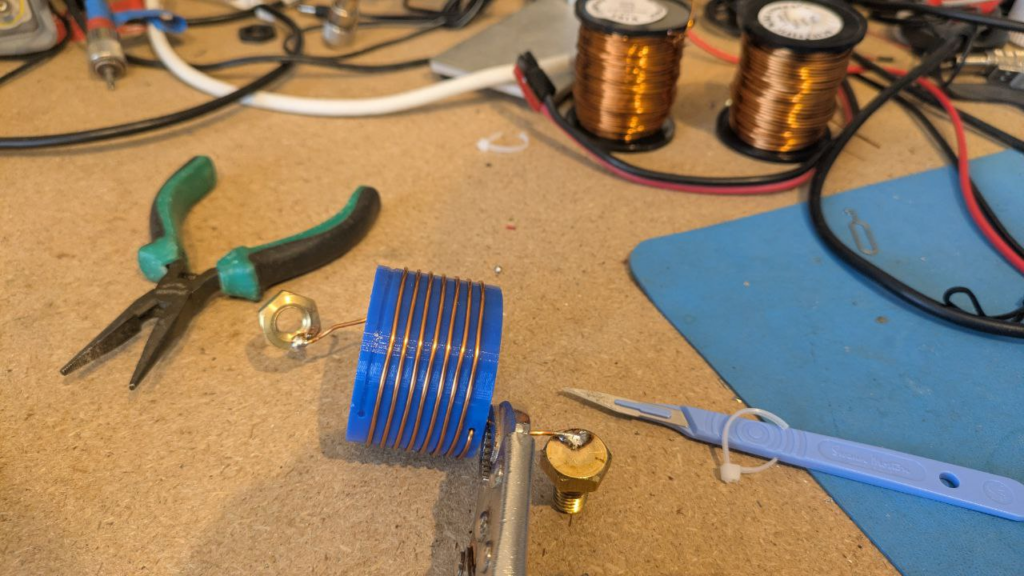
Once assembled internally, a couple of drops of glue can be used to secure the nut and bolt in place – taking care not to get it on the threads – and then to close the case up fixing the ends on with glue.
All images in this section kindly supplied by Rob M0VFC.
Finally, some plastic shrink-wrap or heat-shrink can be used to protect the coil and finish the project.