
You can listen to a WellGood Loop in action on my KiwiSDR in Norfolk or at GB0SNB SDR in Essex. You may also be interested in the PA0RDT MiniWhip project. Since the original publication of this page, I have updated the design to V4 which can be found here.
Introduction & Motivation
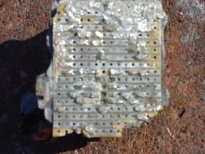
Teardown
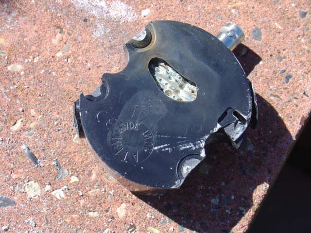
Having had a WellBrook Loop ALA1530 for some time, I accidentally transmitted into it during a moment of madness where I wasn’t using the RX antenna connector. I had been very impressed with the performance of the loop on LF frequencies, such as on 472 kHz and 1.8 MHz, and given the cost of a replacement, I decided to attempt a repair!
The loop is built into a electrical conduit joint box and potted with black resin compound to keep moisture out of the electronics when the loop is mounted outside. However, this made it difficult to repair.
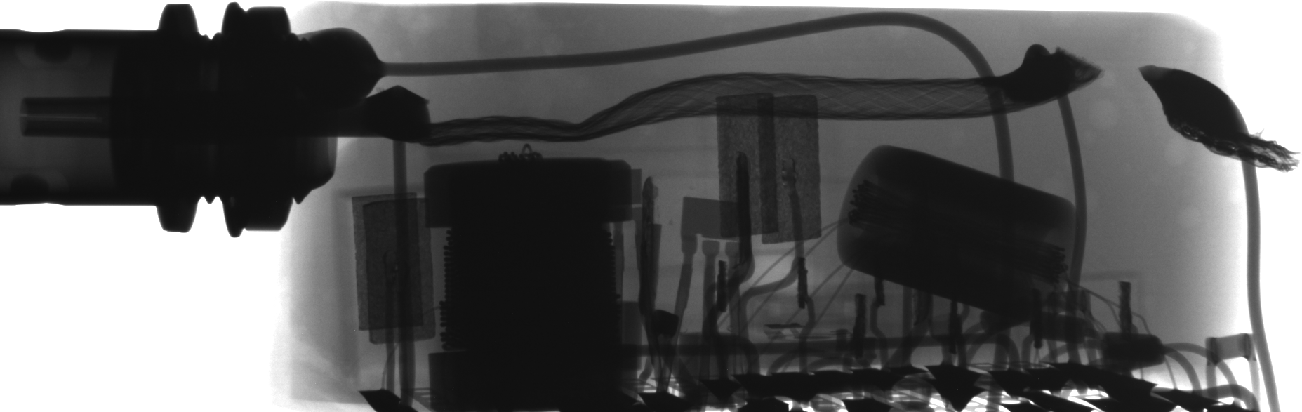
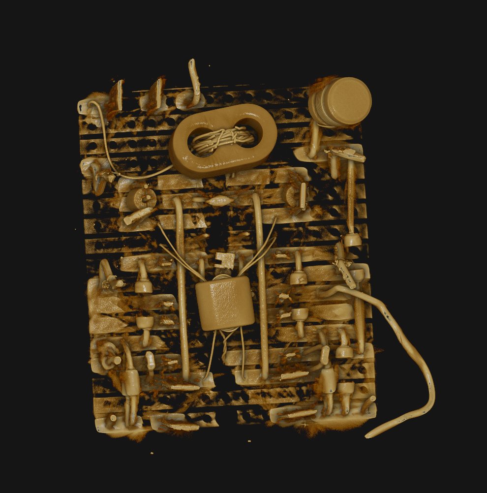
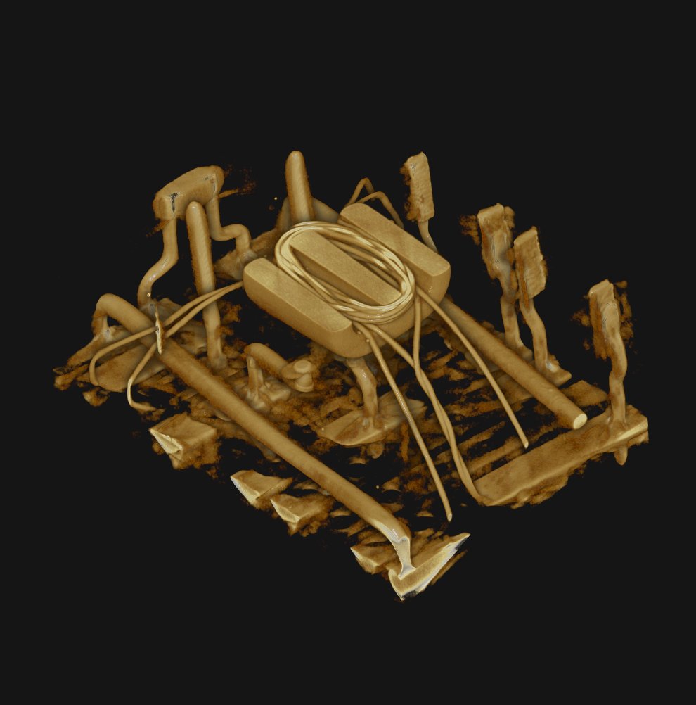
At a local club meet, I was speaking with a friend about my mistake with the loop, and Dave G7UVW who works in an X-Ray lab, offered to x-ray the failed part to assess the feasibility of a repair. You can see these x-rays below. From the x-ray images, it was apparent the device was made on veroboard, with several capacitors, ferrite transformers, and some active transistors.
Since I had nothing to lose, I decided to try and remove the resin compound from the device so I could get at the circuit-board. Various methods were tried, but the most successful was a combination of using a craft knife and pick, as well as warm (around 35C) MEK (methyl ethyl ketone) to dissolve the resin. Over time, we managed to get through, until we could see all of the connections.
As a result of being transmitted into, the transistors were blown to pieces, but the parts in place, and, we were able to read the transistor part numbers as being ZTX327.
In getting to the circuit board inside the resin, many of the wires to and from the transformers were broken, one of the ferrites was cracked, as was the circuit-board, probably due to my haste in getting the resin off. Many of remaining components were worse for wear.
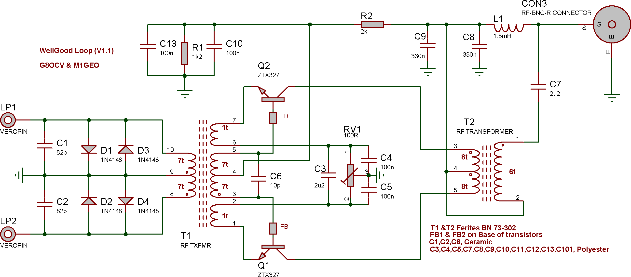
At this point, it was apparent I would need to rebuild the circuit from scratch, and in order to do so, I would need a schematic, since some of the wiring connections were broken. Unable to find a schematic online which matched what I had, I managed to piece the circuit together. As it became obvious that the circuit was balanced, I was able to compare both halves of the circuit to fill in the missing links.
I decided upon using BN-73-302 ferrites based on the graphs for the material, and measurements of AL and frequency response. These are the same size and cover the frequency range quoted for the original antenna design. All the available ferrites in the range were tested.
Theory of Operation
Some time after this page went live, Andy G4KNO brought an IEEE paper to my attention, explaining the original design and theory of operation for the loop:
“Distortion Improvement of Lossless Feedback Amplifiers Using Augmentation,” Trask, Chris; Proceedings of the 1999 IEEE Midwest Symposium on Circuits and Systems, Las Cruces, New Mexico, August 1999.
The pre-print version of this paper may be found on Chris’ personal website here. I have a local copy here (c) 1999 IEEE.
The following patent also contains good background concepts and outlines the fundamental principle of the ‘Norton amplifier’:
“Transistor amplifier with impedance matching transformer“, Norton, D. E.; Podell, A. F.; US Patent 3,891,934, Published June 1975
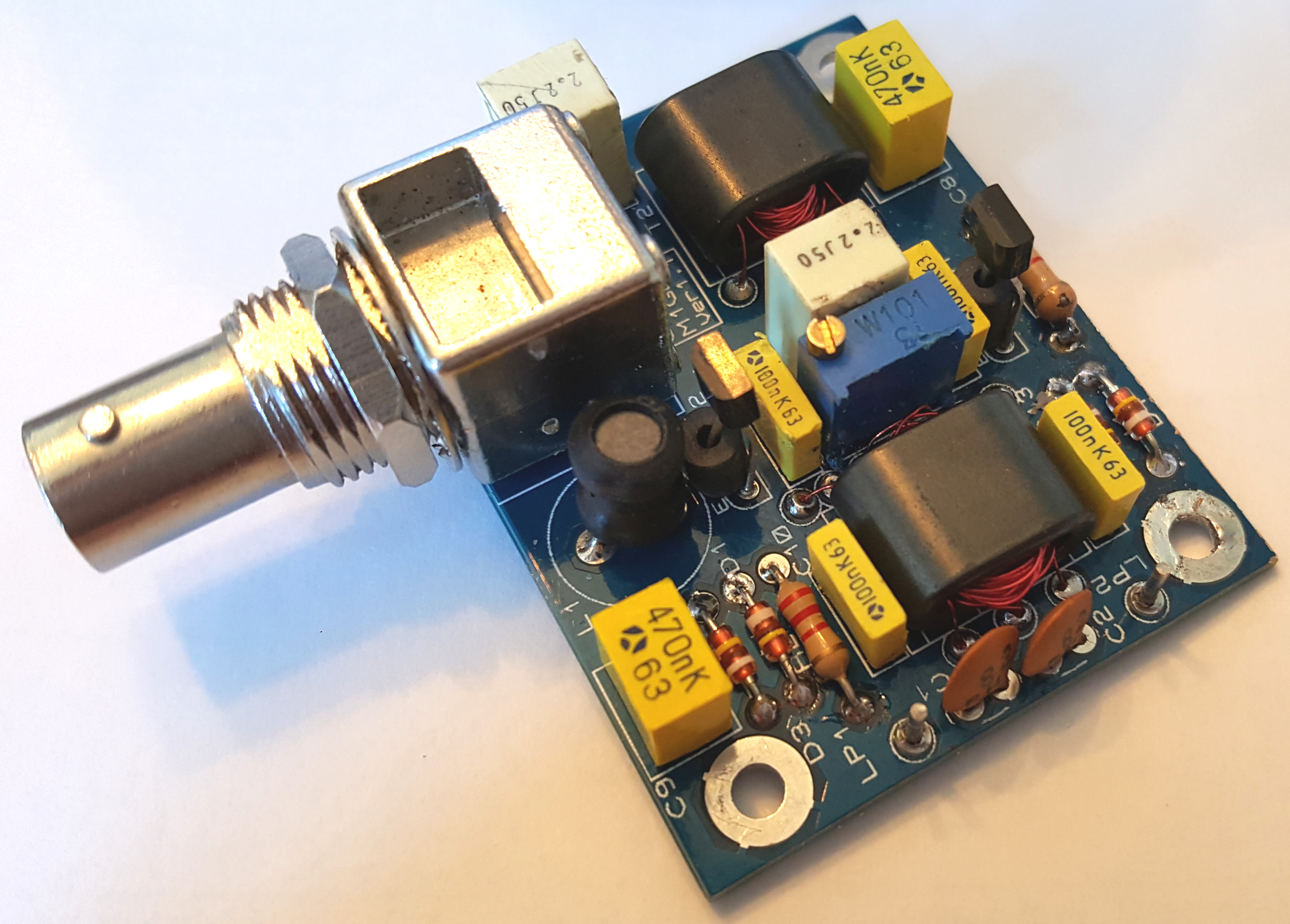
Rebuild
Starting from the schematic we had worked out, we laid out a PCB as I was pretty sure I had the design correct. I added the PCB order onto an existing board order and waited patently.
I made the circuit boards up when they arrived and tested the design which oscillated uncontrollably! This turned out to be due to the phase of the input transformer having positive feedback instead of negative. An easy fix was found, namely, swapping two wires over on T1 (see below).
Another small mistake on the version 1.0 boards was the holes for the BNC connector pins are slightly too small, and may need to be drilled out or pushed in carefully – this wasn’t strictly my fault, since the footprint was the default for BNC connectors in my PCB package. If you do need to do this, be careful that the ground side of the connector is soldered to the top ground-plane on the PCB.
The PCB was designed for the original ZTX327 transistors. However, they are now obsolescent, and expensive, so I have been experimenting with NPN RF power transistors. The ZTX653 is a recommended replacement for new designs. See the section on transistors below.
Finally, with the circuit working as predicted, I connected the loop and observed the functionality of the newly built board to be indistinguishable from the original. I was pleased with the result!
One thing I did notice is that the transistors get warm when in use – I suspect this is due to the high DC quiescent collector current, which keeps the inter-modulation distortion low. The Bill of Materials below suggests some clip-on heatsinks which may help.
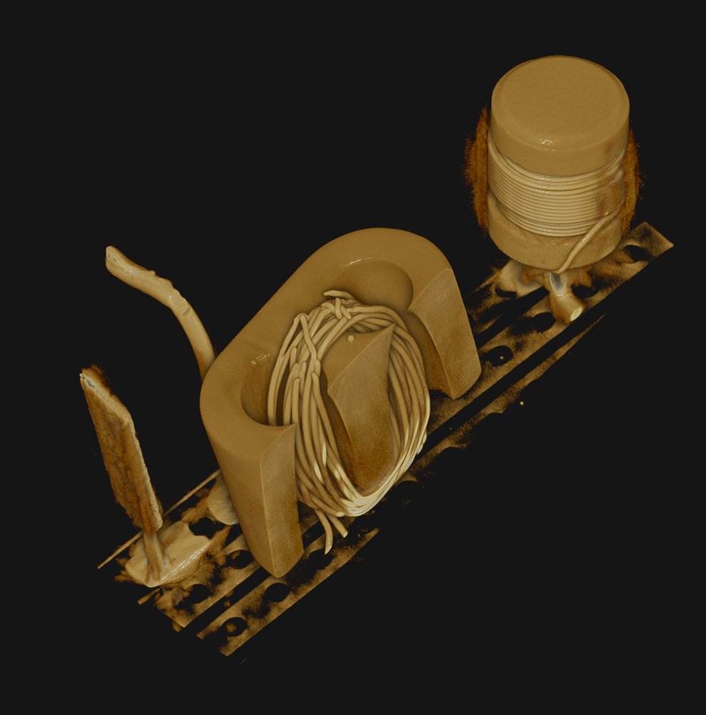
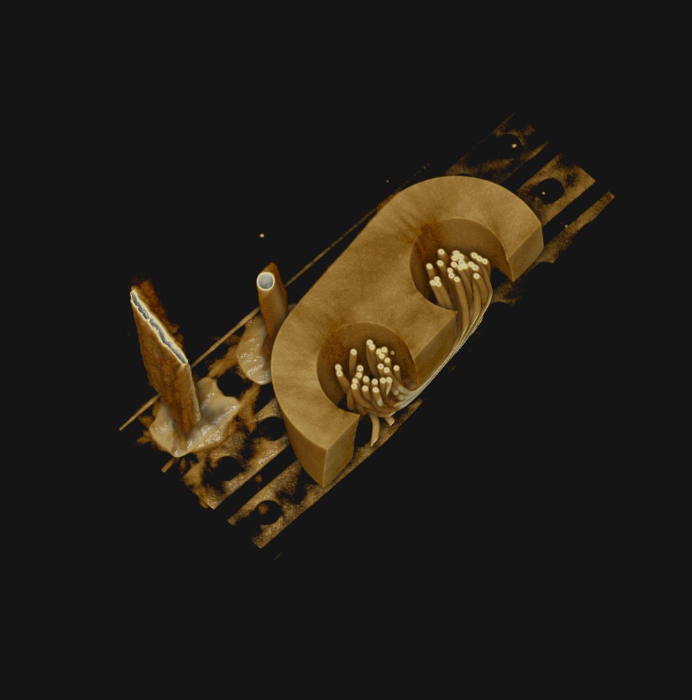
Original Images
Click on images to enlarge. Original X-Ray images provided by Dave G7UVW and Dave M0TAZ.
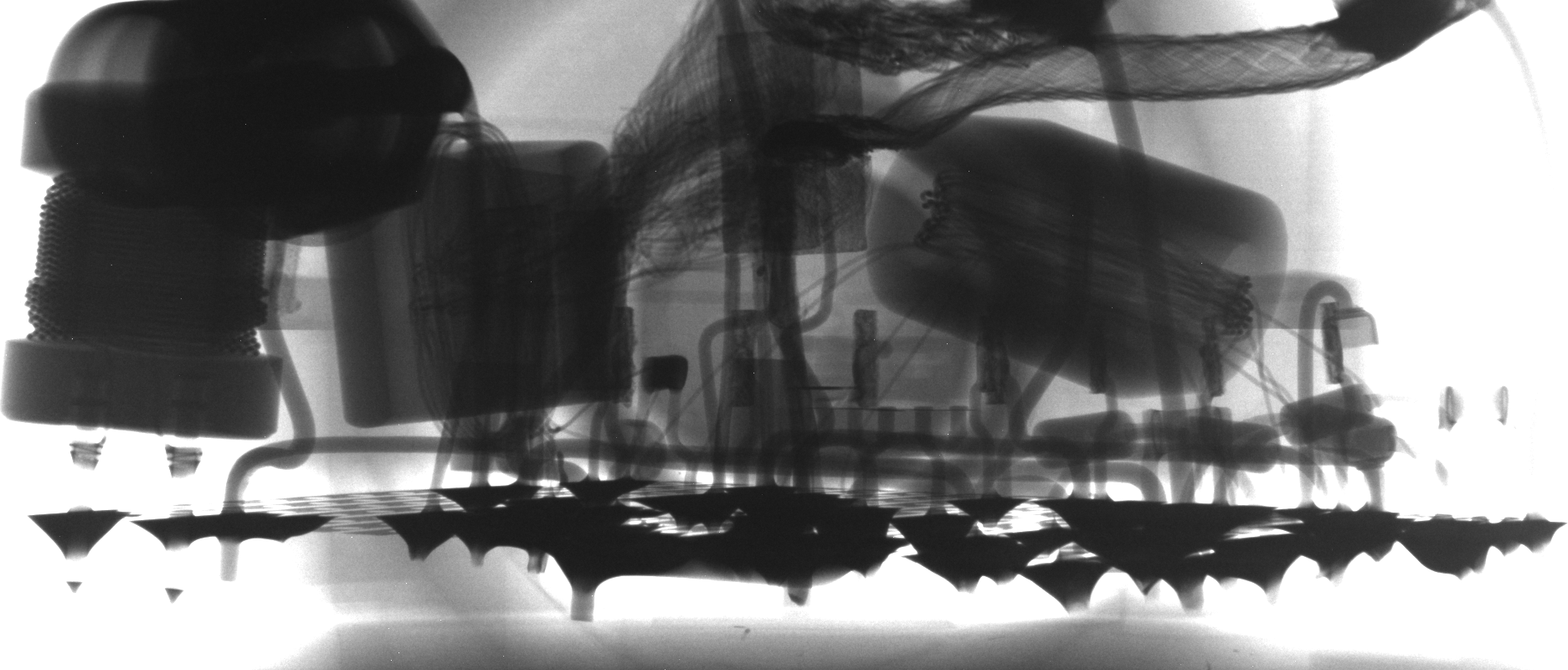
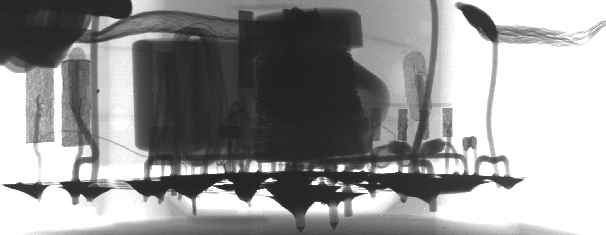
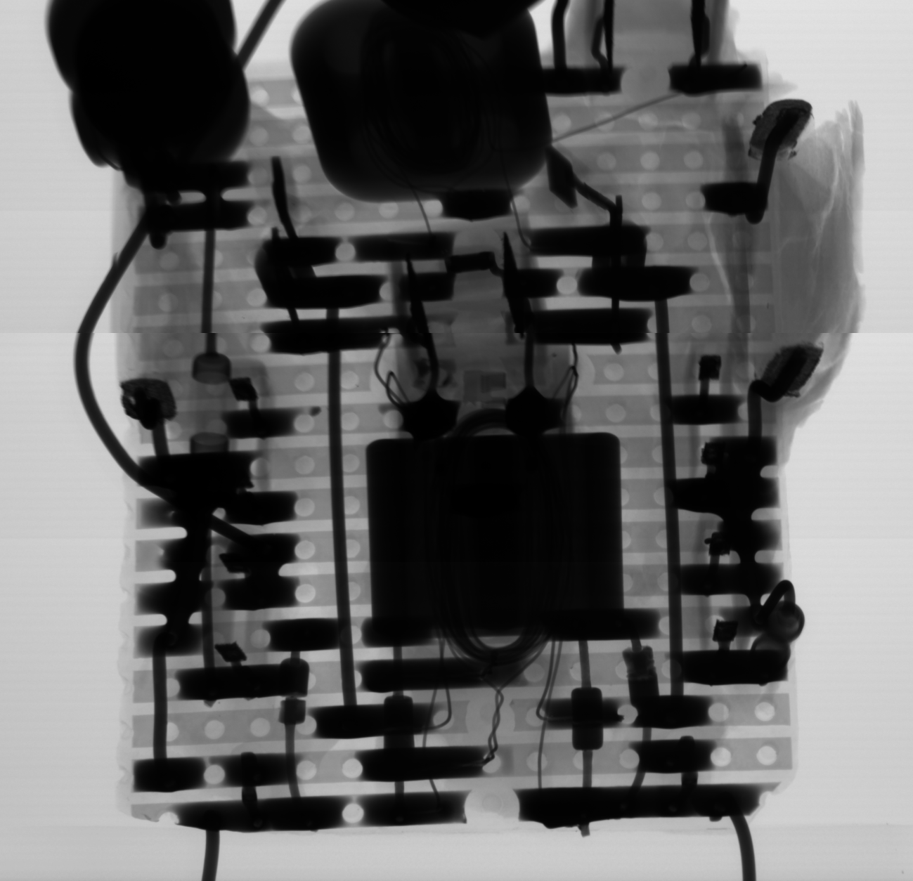
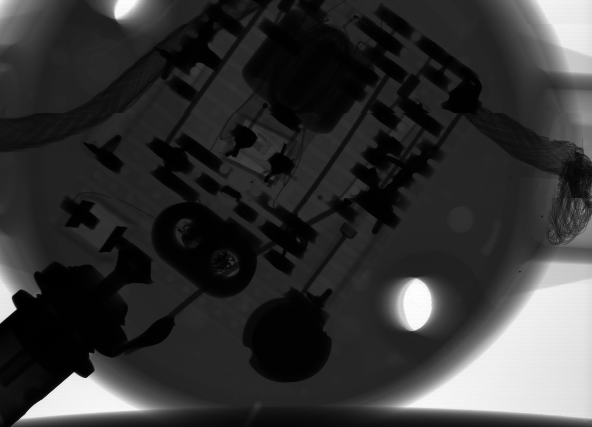
Dave G7UVW went on to share some higher detail images on his Twitter post, the images from which are included below.
 |  |
 |  |
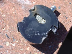
Since this webpage went online, I have been contacted by many amateurs regarding failed loops. Primarily the cause seems to be either transmitting into the receive-only loop, or, water ingress. Derek G3MWO contacted me with pictures of his loop, purchased circa January 2012.
 |  |
| Hole in the resin allowing water ingress | Corrosion on the PCB from water ingress |
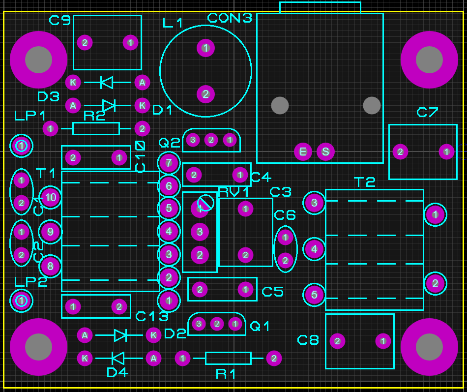
Schematic & Bill of Materials
Loop Board
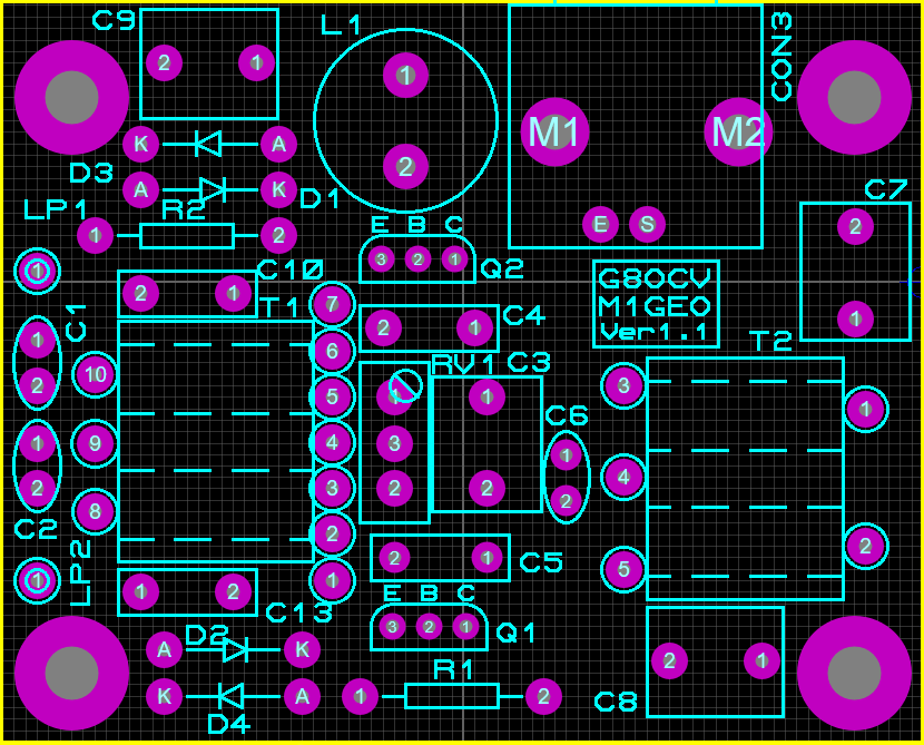
An early version of the PCB had C6 incorrectly placed next to T2. Version 1.1 of the PCB has this issue fixed. In practice, this made no noticeable difference, but will be correct on future versions of the board.
Please note that there is a slight mistake in the the schematic around T1. Follow the instructions for T1 below and all will be fine.
| Component | Value | Count | Supplier & Notes |
| PCB | WellGood PCB V1 (newer version) | 1 | We have spare boards, contact Chris G8OCV. |
| C1, C2 | 82pF | 2 | RS 133-5699 |
| C3, C7 | 2.2uF (must be good quality – in signal path) | 2 | RS 191-985 |
| C4, C5, C10, C13 | 100nF | 4 | RS 538-1310 |
| C6 | 10pF | 1 | RS 538-1146 |
| C8, C9 | 330nF | 2 | RS 312-1582 |
| R1 | 1.2kΩ | 1 | RS 014-8528 |
| R2 | 2kΩ | 1 | RS 014-8578 |
| Q1, Q2 | ZTX327 (original, obsolescent). Others have used 2N3866 or ZTX653. PN2222 ‘works’ at a push, but the FT is a little low and performance will be limited. (See FB1-FB2 and HS1-HS2) | 2 | eBay ZTX327 |
| HS1, HS2 | TO-92 Plug-On Collar Heatsink (60°C/W) – optional | 2 | RS 712-4320 |
| D1, D2, D3, D4 | 1N4148 | 4 | RS 671-5477 |
| CON3 | RF-BNC | 1 | RS 512-1225 |
| L1 | 1.5mH | 1 | RS 675-5232 |
| LP1, LP2 | Loop Connection (1 metre) | 2 | — |
| RV1 | 100Ω | 1 | RS 521-9625 |
| T1, T2 | BN-73-302 / Fair-Rite 2873000302 (see below for winding instructions) | 2 | Mouser 623-2873000302 / JabDog We have these, contact Chris G8OCV. |
| FB1, FB2 | Ferrite bead / Fair-Rite 2643004801 (or similar) (fit to base leg of Q1-Q2) | 2 | Mouser 2643004801 We have these, contact Chris G8OCV. |
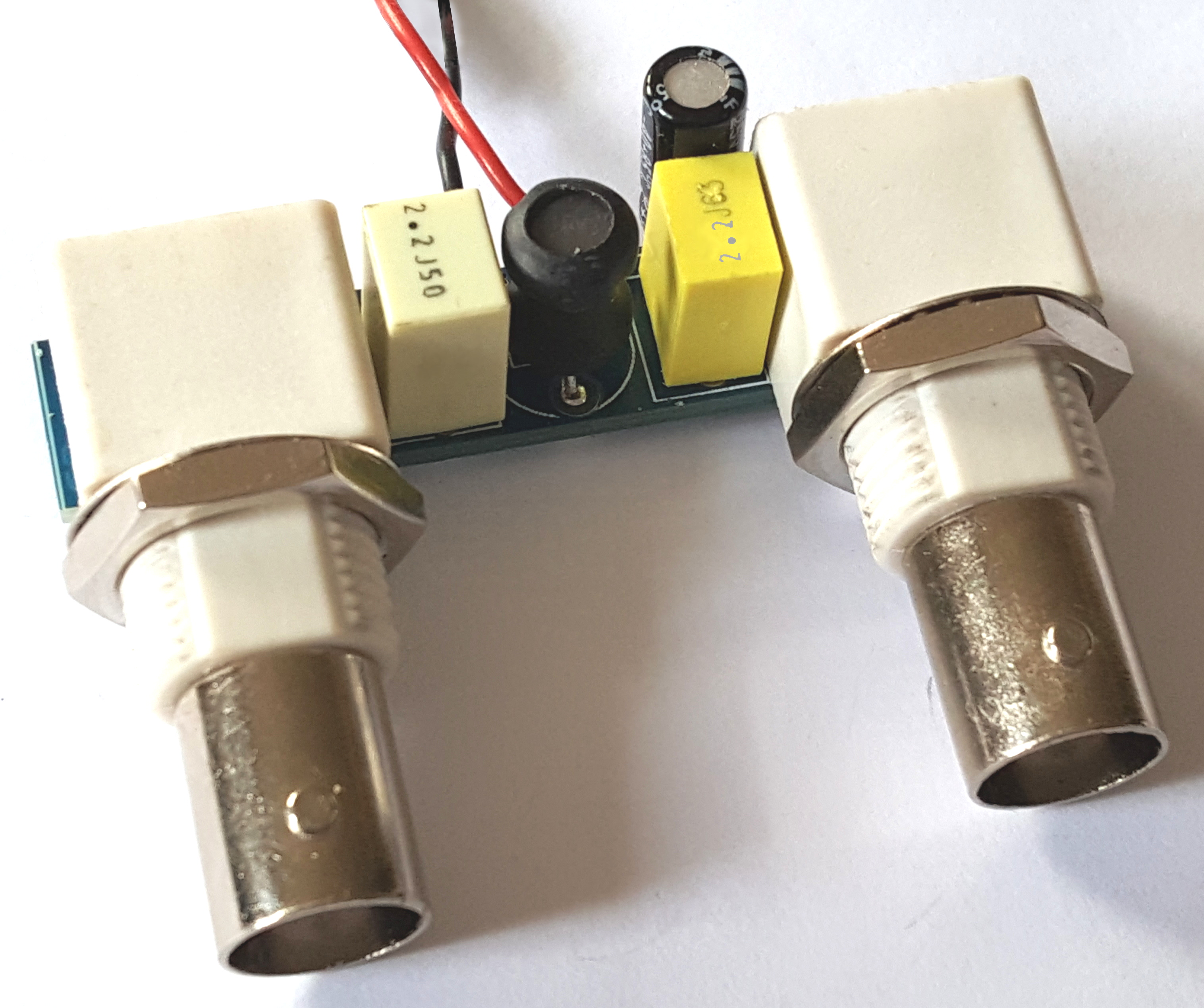
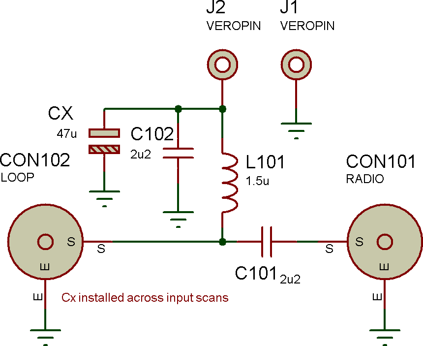
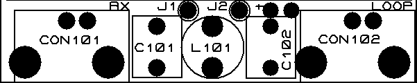
Bias Tee Board
Components for the Bias-T board.
| Component | Value | Count | Supplier & Notes |
| PCB | BiasTee Board | 1 | With main loop PCB |
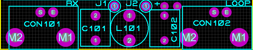
| CON101, CON102 | RF-BNC | 2 | RS 512-1225 |
| C101, C102 | 2.2uF (must be good quality – in signal path) | 2 | RS 191-985 |
| Cx* | 47uF (across power connector) | 1 | RS 747-2137 |
| L101 | 1.5mH | 1 | RS 675-5232 |
Cx* is connected cross the input terminals of the bias tee PCB.
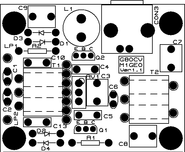
The PCB
I may have spare V1.2 boards; if you are interested in a board to repair a loop, then please email Chris G8OCV. You may also be interested in the pre-assembled V4 design found here.
Version 1.0
Note that on this version 1.0 board, that C6 is incorrectly positioned. It should be installed between the two transistor bases, across pins 3 and 5 on T1. Version 1.0 boards were red in colour.
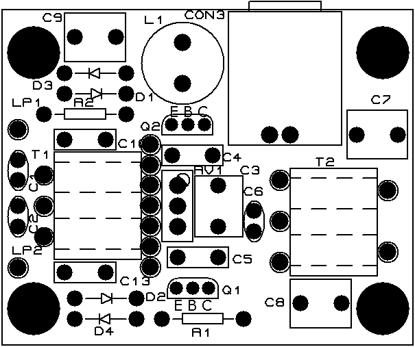
Version 1.1
Due to the capacitor miss-placement on Version 1.0 above, an updated version of the board was produced. These boards are blue in colour. Some spare production area enabled us to also include a Bias-Tee board. The distance between centres for the two bias tee connectors (CON101 and CON102) is 35mm.
 |  |
 |  |
Version 1.2 onwards
Version 1.2 (and up) PCBs are almost identical with V1.1 boards. Some components have moved very slightly to allow more room around the larger capacitors, since this means cheaper (larger) parts can be used.
Build Notes
Winding and mounting transformer T1 is the trickiest part of the build. The making of both transformers is described in detail. You should set the variable resistor RV1 approximately half way before initially powering the board. For the remaining components, it is simply a process of soldering the parts in. The notes describe the recommended approach.
I am aware of the discrepancy between the schematic and the T1 build instructions – this is to make the core easier to wind and solder in. It does not affect performance since the change is balanced by the reversing of the single turn feedback windings. Hence you are advised to work from the winding instructions below.
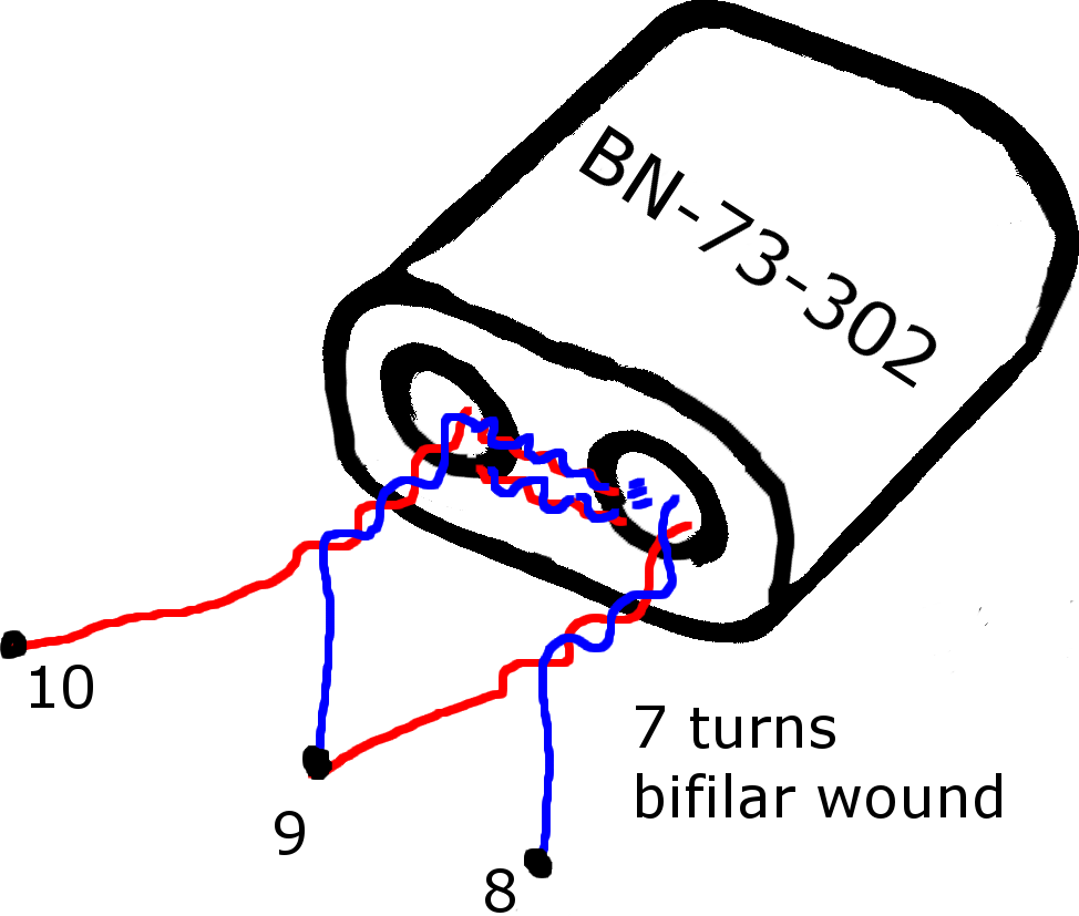
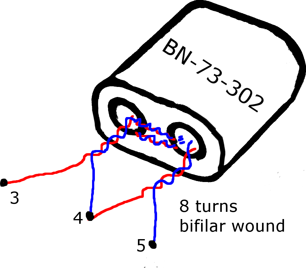
T1
Start off by making some bifilar wire; you can twist two bits of enameled copper wire together. It is often helpful to use two different colours of wire, or use a permanent marker to colour one of the wires in the twisted pair. If you can’t colour the wires, it’s easy to sort them after winding using a Ohm-meter. I’ve used 0.25 mm diameter enamelled copper wire as I had that available, but this not too critical, as long as all of the windings fit on the cores. The original had 0.2 mm diameter wire.
The first job is to wind the loop (input) side of T1. Wind 7 turns of the bifilar wire around the BN-73-302 core, creating a centre-tapped point, as shown below. The numbers refer to the solder pads in the colour placement diagram.
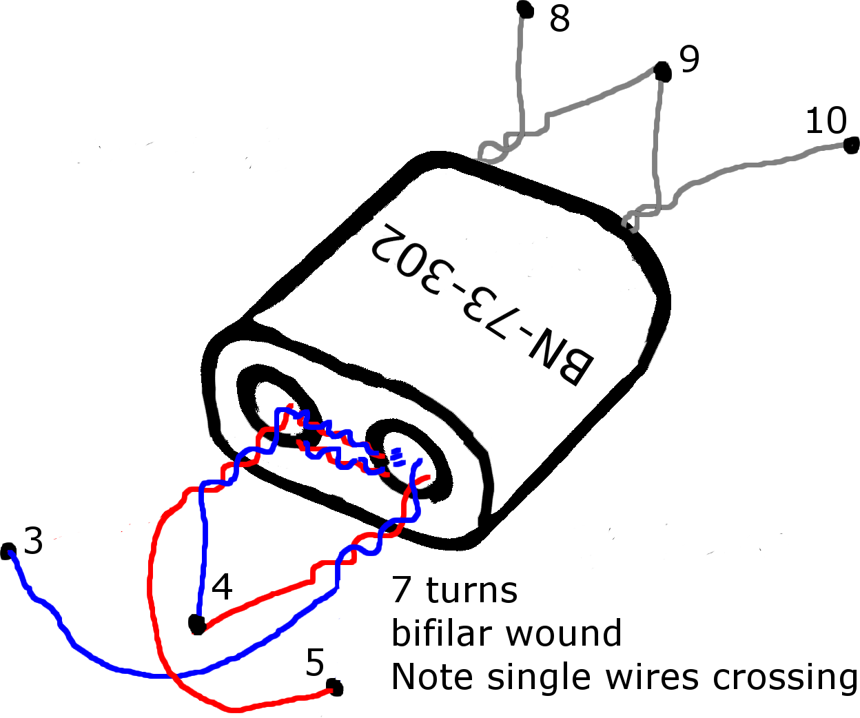
Flip the core around and repeat the process to make the first of the secondary windings for T1. As with the primary, two of the wires are connected together to form the centre-tap and will connect to pin 4. The two remaining wires need to be crossed to prevent the circuit from oscillating.
At this point, it may be easier to mount T1 transformer to the PCB and add the two single turn windings on afterwards – with a binocular core, one turn is a ‘U’ loop through both holes. These last two windings are made from a single piece of wire (not bifilar), which go in through one side of the core, and out of the other. One of the windings goes from pin 1 to pin 6, and the other between pin 2 and pin 7, as shown.
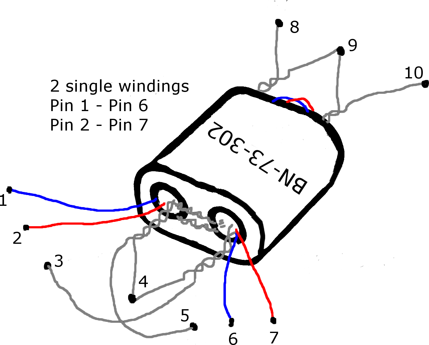
At this point, you should have transformer T1 mounted correctly. If you experience high frequency oscillations (15-30MHz) from your build, adding an extra feedback turn, i.e., passing ends 6 & 7 through the core once more to end up at the same point, usually helps. This is very occasionally the case when transistors have an exceptionally high HFE.
T2
Using the same bifilar wire as you made for T1, wind 8 turns for the primary of transformer T2. Separate the two strands and create the centre-tap as before, shown below. As with T1, I used 0.25 mm diameter enamelled copper wire but the original was 0.2 mm diameter.
The secondary winding of T2 is 6 turns of standard (single core) enameled copper wire, as shown below.
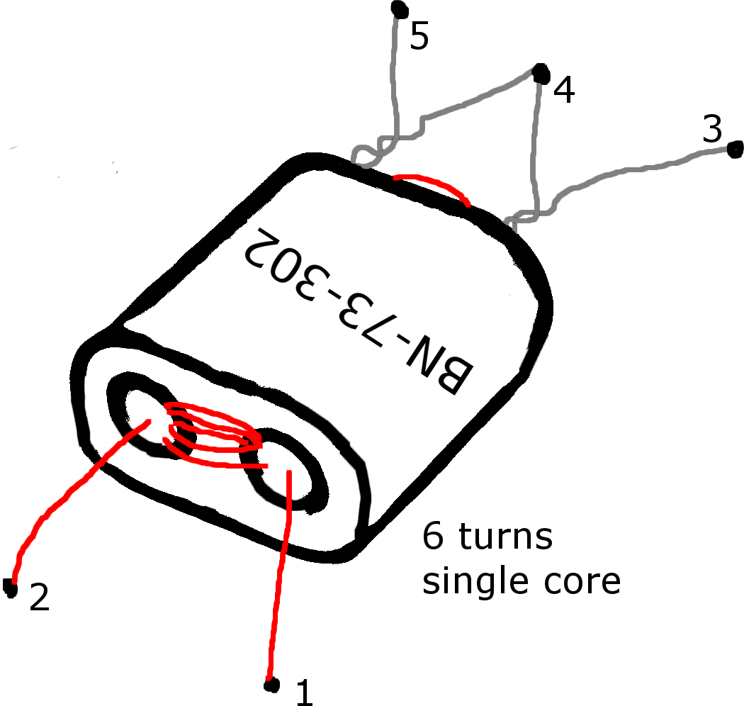
Mount this to the PCB and transformer T2 is also complete.
Transistors
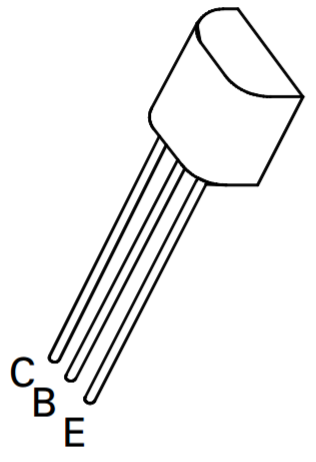
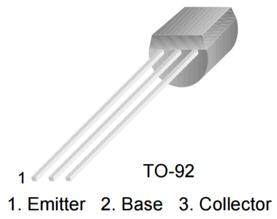
The transistors used in the original design were ZTX327, and so this board is designed to fit those. These are now obsolete and are quite expensive to acquire from sources such as eBay. A ZTX653 has a matching pinout with suitable characteristics, and would be a direct drop-in replacement for the ZTX327. Preliminary tests were done with an MPSH10, but the pinout is different, and so require some tweaking to fit to the board. The original ZTX327 transistors had a hFE-min of 15. It is important not to have too high forward current gain (hFE) on the transistors, as this will disturb the correct biasing of the transistors. The pinouts are shown below. Dave GW3WCV writes in (see Feedback section below) to say that he had success with PN2222A devices but the 2N3866 was better.
After considerable testing, I have found that the PN2222 isn’t up to the job and the performance suffers as a result. My recommendation is to use an small RF power transistor as they yield the best results.
Note that the transistors will get warm when the circuit is in use – this is due to the high quiescent current through the transistor pair, which maintains a high inter-modulation level. The Bill of Materials section above has clip-on heatsinks to help with this should you choose.
RV1
The variable resistor should be set to approximately half way before initially powering the loop. Once you have built the board, you will need to balance the current through the two transistors. The easiest way to do this is to adjust RV1 to minimise the potential difference across C3. Ideally this should be 0 mV, or as close as possible, within a few milli-Volts.
Tacking two wires to the back of C3 allows you to easily adjust RV1. Remove once you are happy with the balance.
Remember that the transistors Q1 and Q2 will get warm, especially if they are not balanced. This heating greatly affects their HFE (gain), meaning their temperatures will effect the balance. You should adjust the balance slowly, allowing the devices to heat up/cool down, as you are adjusting. I found blowing gently on the PCB between adjustments helped the temperature to settle more quickly
CON3
The BNC connector is used to connect back to the shack. The ground side connects to the top copper. On V1.0 boards, the drill holes for the BNC connectors may be too small and thus require drilling out. V1.1 onwards do not need any modifications here.
Capacitors
Capacitors C1, C2, and C6 are ceramic disc type capacitors. The remaining are polycarbonate, polyester, or similarly good quality – certainly not ceramic. This is especially important in any RF signal paths (C3 and C7), where ceramic capacitors are not of high enough quality. The same is true for C101 on the Bias Tee board.
Depending on the exact capacitors you use for C3, C7 and C101, you may need to do some fine fettling to get the components to fit.
CX on the bias tee can be connected across the input terminals.
The remaining parts
The remaining parts can be fitted to the board as standard.
Power
The loop is powered by a bias-T, which injects DC along the coax. The original bias-T was not examined, but, we have used a 2.2uF capacitor such as C7 and the same 1.5mH inductor such as L1. The loop should be fed with a nominal 12V supply, and draws around 140 mA. It is important to power the board with a sharp rising 12V supply – gradually winding the voltage up is known to cause oscillation – this behaviour also occurs on the original design.
The Loop
The loop on the original antenna was made using RG58, with the outer screen used as the loop, and the inner conductor not connected. This was then supported in a plastic pipe. Others have reported that their loops were made with a clip together metal ring. The diameter should be around 1 metre, and thus around 3.14 metres of material is needed to create the loop circumference. Ideally, you want for the loop conductor to have a largish diameter. A tube or coax screen will outperform a small piece of wire.
I have used 8mm aluminium bar with good success, either with a metal rolling machine to achieve a ‘perfect’ circle or using a simple jig to bring the ends together. Others have used coax (both RG58 and RG213 styles) supported in a water pipe which gives good results. Another report has been to use a metal hula-loop to create the loop, with extra screws in the joins to ensure a good electrical connection around the loop. Such hula-hoops are often sold on sites like as eBay or AliExpress as “weighted fitness loops” or similar.
Feedback
Since offering surplus boards to help others with restoring damaged loops, I have had feedback from several people. Some of which contains useful information:
Dave GW3WCV
Dave wrote to me and said the following:
Hi George
Just a line to let you know that the build of the amps (I had 2 boards from you) went very well indeed and your instructions and parts lists were spot on! I built them using the ZTX653 transistors you suggested, they worked great but found the frequency response dropped off dramatically above 5MHz. Swapping them for some PN2222A’s helped a lot (10dB more on 28MHz) but got 14dB more by using 2N3866 and the same result, but a bit less noise, from some 2N5109’s. Bias adjusted for 50mA through each transistor. They are a bit big for the board though so have had to move one leg of the choke to the board edge.
Hope things are good with you, many thanks once again for the great project.
73, Dave GW3WCV
Dave went on to add a further update a few days later:
Hello George
Have done a bit more experimentation and found the input Z rises dramatically above about 10MHz. This makes the gain figures I originally obtained a bit too high at the HF end since the output Z of the generator is 50 ohms. However, the replacement transistors still do make a significant difference for those using the amp above 7Mhz. Sweeping carriers on 80m traced to my Alinco DM-330MW SMPSU. Fitted another choke wound on a toroidal ferrite core into the supply from the SMPSU to the Bias T board fixed the drifting carriers. Despite living very close (4km) to Wenvoe with its massive RF output I have had no overload/crossmod problems with the amp. Very pleased with the result. Many thanks again.
73, Dave
Derek G3MWO
Derek G3MWO wrote to me to show water ingress present into his loop and the attached pictures which can be found at the top of this page (here and here). He writes: Hi GeorgeI have been sent a copy of your excellent article on the Wellbrook Loop by David G3MPN of Wymondham.He had one that failed after a short time and was replaced by the supplier. David then gave me his old loop to “play” with as i was suffering severe interference on 160 metres. I did a postmortem on it with a hammer and chisel to get some idea of what laid inside the box – which was a truly destructive process!! Clearly the Veroboard need a couple of 6 mm breathing holes for the air under the board to escape as the resin was poured in!! I found a large air filled void under the board where the copper tracks, being unprotected, were severely corroded – no doubt as a result of the acetic acid generated by the resin curing process. I rebuilt the amplifier from a circuit found on the internet which was a fairly simple balanced design — but it does work, giving a good noise reduction relative to the wanted signal.I attach a picture of my findings for your interest.RegardsDerek G3MWO
Everett N4CY
Everett N4CY wrote to me to say that he had previously studied loop antennas for an article he wrote for Medium Wave News, which is linked to here.
Jim G3KAF
Jim wrote to me to express his delight with how his repaired loop worked:
I have today finished constructing the loop and it is excellent. I am delighted to let you know that the Well Good Loop is a great help. George, many many thanks for making your board available to me. I am sure other hams suffering high noise levels like myself would welcome the opportunity to construct the amplifier and T Bias boards.
Giovanni IZ5PQT
Giovanni and I had a chat via email about the loop and how it compares to the PA0RDT MiniWhip:
Hi George, just to tell you that the loop works very well. From some preliminary comparison tests on SW with the Mini Whip the loop is clearly better under 9 MHz. The Miniwhip has more gain from 9 MHz upwards. But where the loop really shines is on MW. I have many channels which cannot be heard with the miniwhip (or with a longwire) because there is just noise, whereas they are perfectly received with the loop. Thank you for having made the PCB available and for the super clear instructions for the transformer winding: truly an excellent job. My QTH is within 10 km from a 50 kW MW transmitter. Absolutely no intermodulation problems!
Jonathan G8DJN
Jonathan emailed me noting the directionality of the null was impressive
I have just built and now using one with very good results on the lower bands. The ability to null/suppress local noise has made 40m and down useable again!
Matthias DD1US
Matthias performed some testing of the loop using an AirSpy HF+, although he used slightly different capacitors than those specified in the signal path. Matthias’ report can he found on his website.
Credits
This project was made possible with the help of the following people.
You may also be interested in my PA0RDT MiniWhip project.