
Overview
In the last few weeks, I have stumbled into a few projects that required a Bias Tee. That is, a device for feeding power (DC) along a transmission line along with a signal (AC). This technique is very common and is used to power LNBs (those little blobs at the centre of satellite dishes) and mast-head pre-amplifiers commonly used on VHF/UHF antennas to overcome cable losses. One example is the DG8 144 MHz mast-head preamp (homebrew by me, design by Ian White GM3SEK).
To avoid running a separate power cable to the mast-head pre-amp or to the LNB, I decided to design a Bias Tee. Something that will inject the DC on to the feeder and also separate the RF signal from the DC power for feeding into my radio. Since I use these antennas for transmitting as well as receiving, it is important to have the power disabled when the radio enters transmit mode, so that the mast-head electronics enters bypass mode.
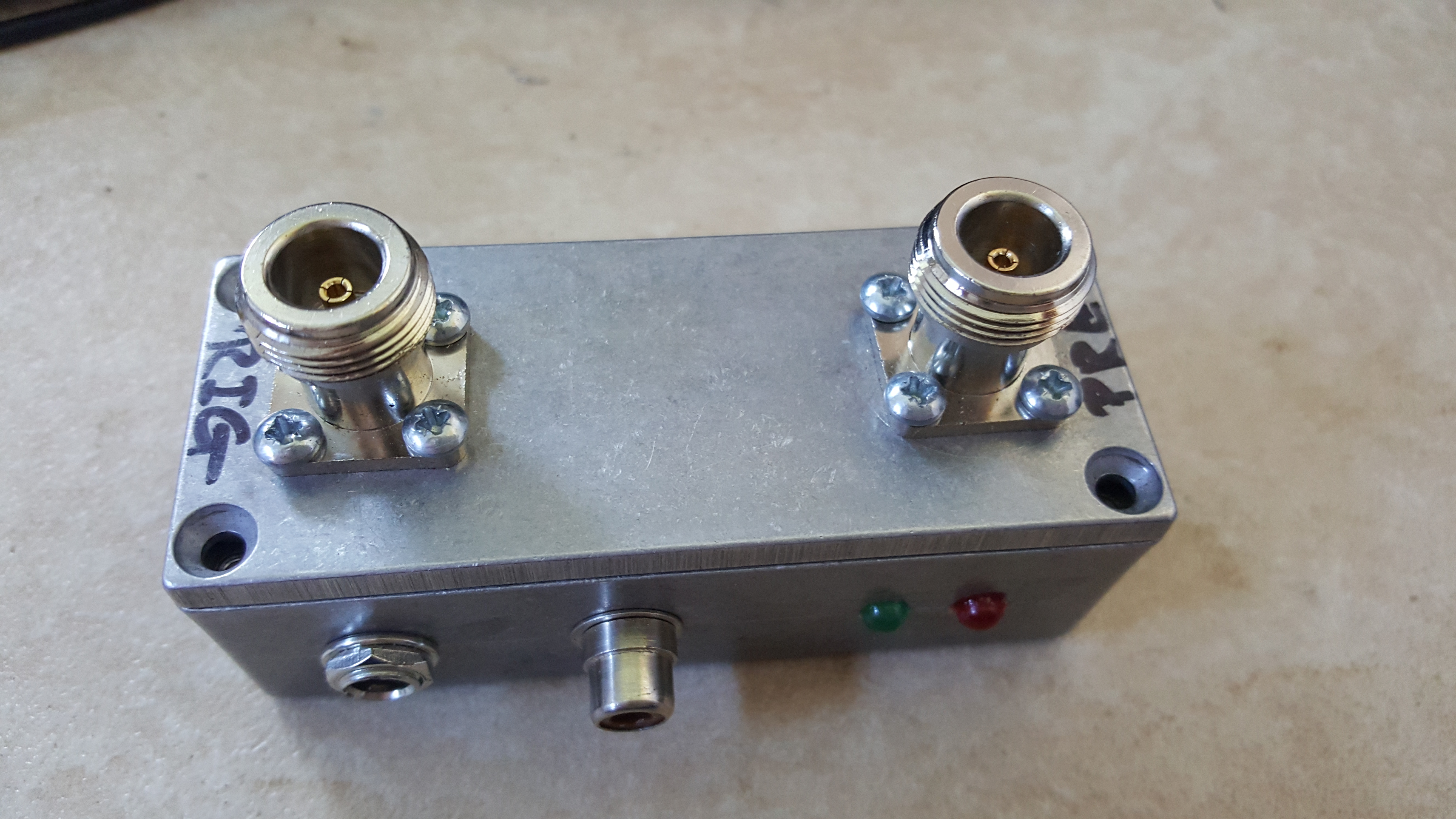
Below is the first practical version, boxed, with two N-type RF connectors, a RCA (phono) connector for PTT input, and a 3.2mm power connector.
The Design
It’s easy to design something that meets this basic criteria. I had considered buying something that would work but these didn’t offer PTT switching, which I deemed important for my application. I decided to start designing my own. I would need:
- An inductor will have a low impedance to DC, but a high impedance to AC. This will inject the DC power.
- A capacitor exhibits the reverse frequency characteristics; high impedance for DC, and low for AC. This will separate the AC signal.
- Some electronics to control power to the preamp in an automatic way, based on the PTT input connection.
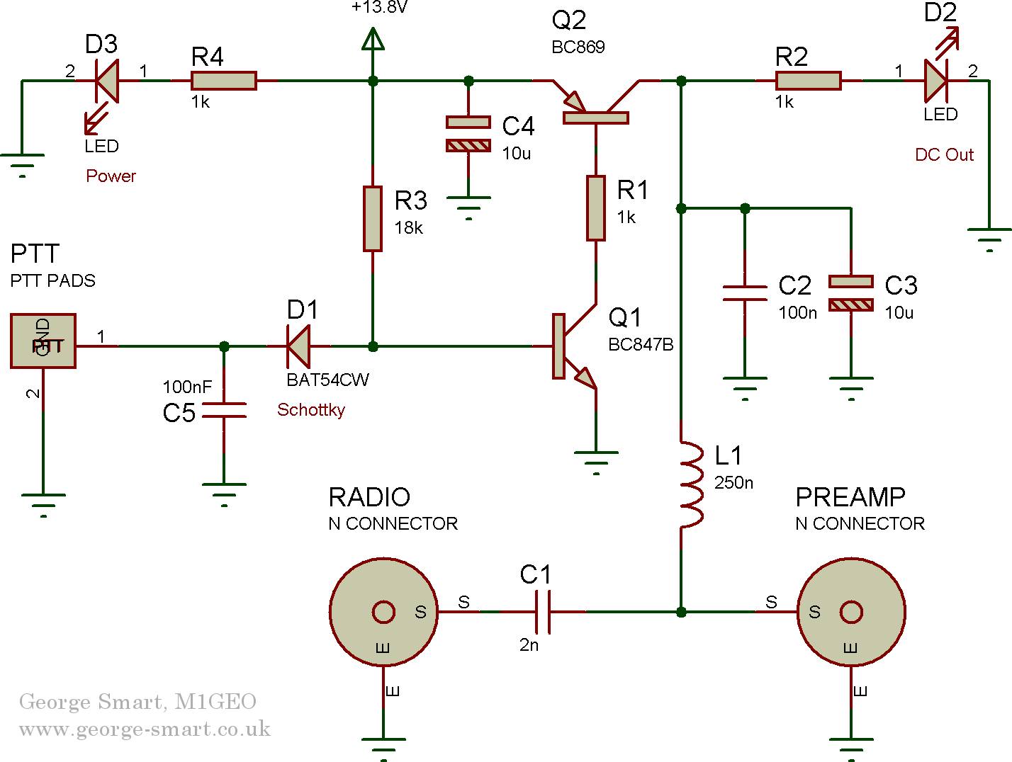
By selecting the values of L (inductor) and C (capacitor) correctly, we can design for any impedance ratio we like. I have gone for an impedance ratio of 100 times at 144.3 MHz, so  . To keep the size of inductor sensible, I used a known good value from the original DG8 design, 250nH. Some extra capacitors will provide a bit of extra AC filtering after the inductor.
Early versions of this project used a relay for PTT switching. However, I decided against for later versions because the relay takes some time to operate. Ideally the preamp should be switched off as soon as possible when the transmitter is activated. The transmitter has a small delay between activation and RF output, so the sooner the preamp is disabled, the less likely it is for an issue to occur. When the PTT signal pin is grounded, the bias tee DC output should be disabled.
2 LEDs are provided to give a visual feedback of the signals. A polyfuse can be used to protect the control electronics from short circuit.
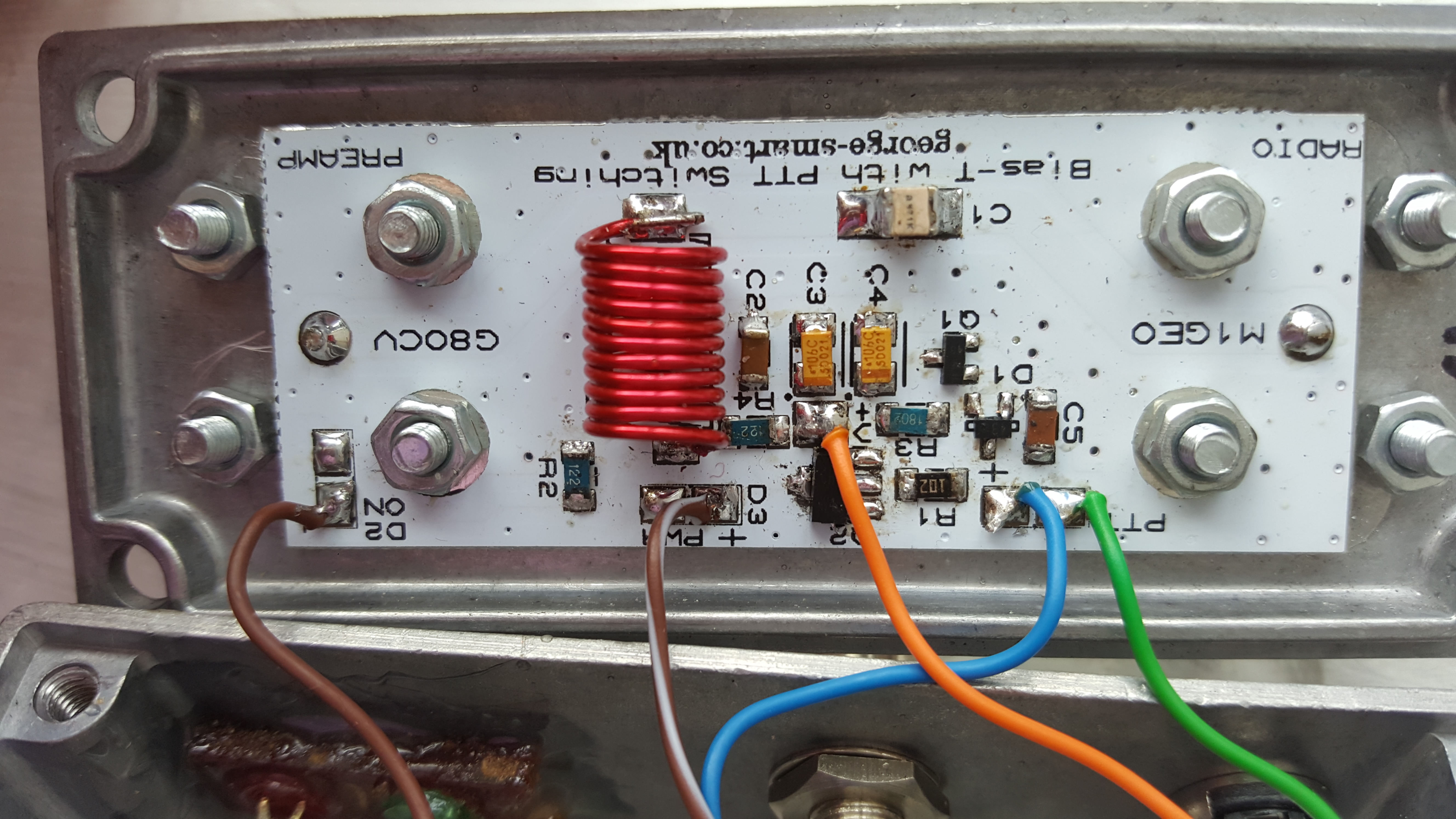
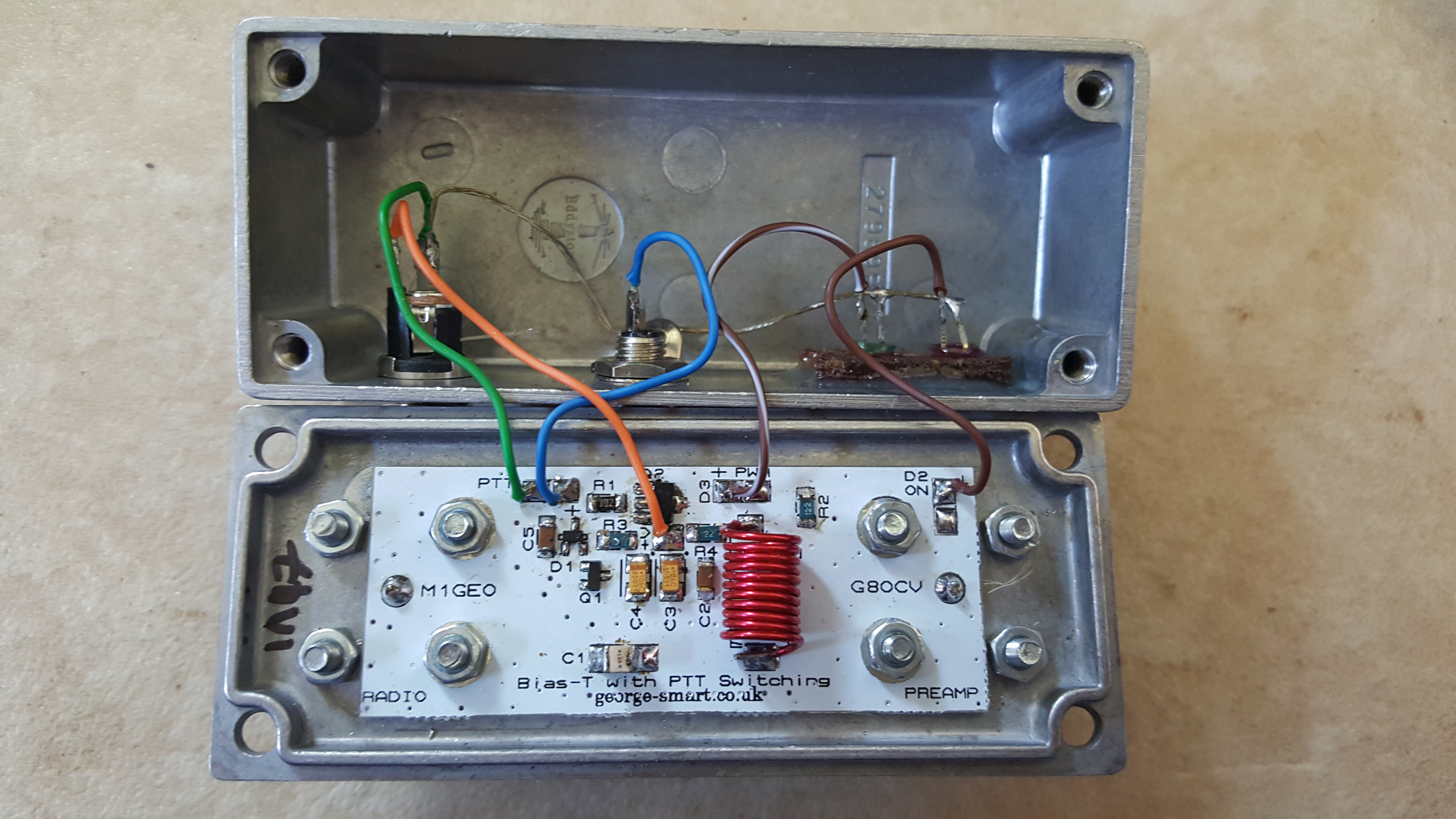
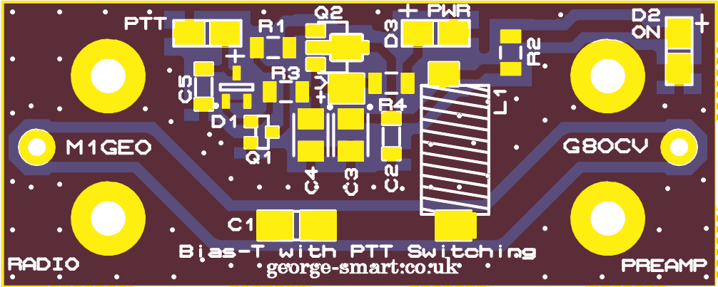
The design was made surface mount design to fit on lid of Hammond Manufacturing 27969PSLA (Farnell 301516) diecast Eddystone box. A 50 Ohm micro-stripline provides a reasonable impedance match through the bias-tee. This design has been tested at 400W (the UK maximum power limit), although testing at higher power levels remains to be done.
The box is easily drilled on the top using the PCB as a template or more accurately using vernier calipers. I chose to mount the LEDs, power and PTT connectors on one side, but you can choose.
Schematic
The below schematic matches the PCBs above. The design is simple as leaves room for improvement. A future improvement to work on is fold-back current limiting. At present, a polyfuse should be fitted in the +13.8V supply line. It is not shown in the pictures above (as they hadn’t arrived at that time). This may protect the series pass transistor, Q2, in the event of a DC-short antenna being connected to the coax in place of the preamp.
PCB
The PCB design above shows the parts layout for the bias tee. The under side is a ground-plane. The PCB has been swept on the VNA and offers a good frequency response from 50 to 1296 MHz. The frequency response is limited by the inductor, L1. For lower frequency (HF) use, you may try using a ferrite choke in place of L1. I may have spare PCBs available, so if you are interested, please contact me.
Bill of Materials
List of materials for the bias tee PCB as presented. The supplier indicates where I brought my parts from. They may be available cheaper elsewhere.
| Component | Value | Count | Supplier & Notes |
| PCB | PTT switched bias tee PCB | 1 | If interested, contact me. |
| BOX | Hammond Manufacturing 27969PSLA diecast Eddystone box. | 1 | Farnell 301516 |
| CON1, CON2 | RF N-Female 17.5mm flange mount | 2 | Easily available on eBay |
| CON3 | 5.5mm x 2.1mm DC Female Chassis Power Socket | 1 | Easily available on eBay |
| CON4 | RCA Phono Chassis Socket (PTT input) | 1 | Easily available on eBay |
| D2, D3 | Power and status 5mm LEDs for indication | 2 | Farnell 2335725 |
| R1, R2, R4 | 1kOhm (1206) | 3 | Farnell 1576629 |
| R3 | 18kOhm (1206) | 1 | Farnell 2447472 |
| D1 | Schottky diode BAT54CW (SOT-323) | 1 | Farnell 1081193 |
| Q1 | BC847B NPN (SOT-23) | 1 | Farnell 1081232 |
| Q2 | BC869 PNP (SOT-89) | 1 | Farnell 1757901 |
| C3, C4 | 10µF 20V tantalum (1206) | 1 | Farnell 2112919 |
| C2, C5 | 100nF 50V ceramic disc (1206) | 1 | Farnell 1759361 |
| C1 | MC22FA202J-F 2nF 100V (2220) [see below] | 1 | Farnell 2361774 |
| L1 | 10 turns, 1mm enameled copper wire, close wound on 5.5mm drill | 1 | – |
C1 is the main RF bypass capacitor and is specified at 2nF 100V. it should be mounted sideways to minimise interaction between the capacitor plates and the PCB groundplanes. The Cornell Dubilier part specified is rated to an AC RF current of 10A. In theory, at 50 Ohms, this equates to 5kW. The PCB track has been tested to 400W, although it would likely handle 1kW (4.5A at 50 Ohms), it has not been tested. You may of course swap this for something less ambitious if you require, but the capacitor must be suitable for RF current. ATC or Cornell Dubilier parts are known suitable.