Category Archives: Engineering

Symmetricom GPSDO Enclosure

While tinkering with a homebrew GPSDO project, I spent a bit of time searching the depths of the internet for information and parts for my project. I found a PCB for a Symmetricom GPSDO (specifically the Symmetricom 089-03861-02 as per the PCB silkscreen in my case, although the firmware reports itself as 090-03861-03). The board was cheap because the OCXO was missing – I suspect it had aged beyond where the error voltage range was specified, making it unusable. But the board was around £15 GBP delivered from AliExpress, so I took a chance on it based on the fact it had a Furuno GT-8031F GPS receiver which is a GPS module specifically designed for timing applications which “delivers highly accurate GPS timing”. The module also had a CPU (Renesas F2317VTE25V-H8S/2317) with accompanying flash and RAM ICs as well as a Xilinx Spartan-3 FPGA (XC3S200).
Besides the missing OCXO module, my board worked perfectly. I was able to piece most of the information together from the following two resources:

I saw that some people had put their units into Hammond Manufacturing project boxes, and that gave me a few ideas. It would be nice to box the unit up with some ancillary electronics to share the UART (57600 baud, 8N1) over Ethernet TCP/IP. However, my experience of UART to Ethernet modules has always been poor and friends reported similar, so I opted for an FTDI-based USB interface (namely the FT232RL, as the cheapest/easiest part during the chip shortage of 2019-2022). I was tempted to use a Maxim MAX232 device to perform the necessary conversions, but, in the end opted for two NPN transistors – a bit hacky, but much cheaper. I may well come back to the Ethernet option in the future.

The carrier takes 5V at around 2A input on a 2.1mm x 5.5mm DC power socket, a USB-B connector and holds five LEDs: four main LEDs from the GPSDO (which are connected to test-points on the PCB, I can’t find the LED signals on any connector), plus one LED from the FTDI device showing USB activity.

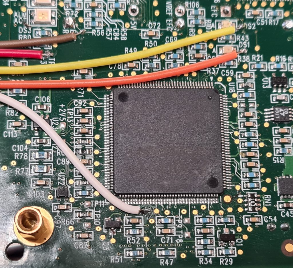
The image below shows where the LED signals are taken from. For reference, the big IC in the centre is the Xilinx Spartan FPGA:

The LED signals are all common anode, fed from +3.3V taken from the board. The LEDs are fed through a resistor, and the individual cathodes connect back to either the CPU or FPGA through another of the wires:

  • RED: +3.3V supply used to power the LED anodes
  • BROWN: Alarm
  • WHITE: Activity
  • YELLOW: Heartbeat (DS2)
  • ORANGE: Error (DS1)

There are two other LED signals (DS3 and DS4) which aren’t connected.

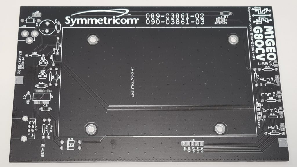
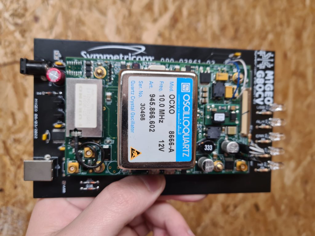
From here, I created a carrier board which had the correct mounting holes for the Symmetricom module, and offered front LEDs to show status, an easy 5V interface and a USB-UART interface to the module control port. The final board looks as below:
With the module fitted, the board looks more like the following. Note, this was an earlier version of the PCB:
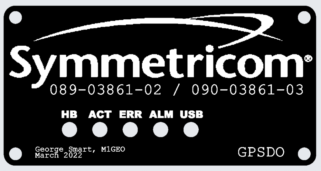
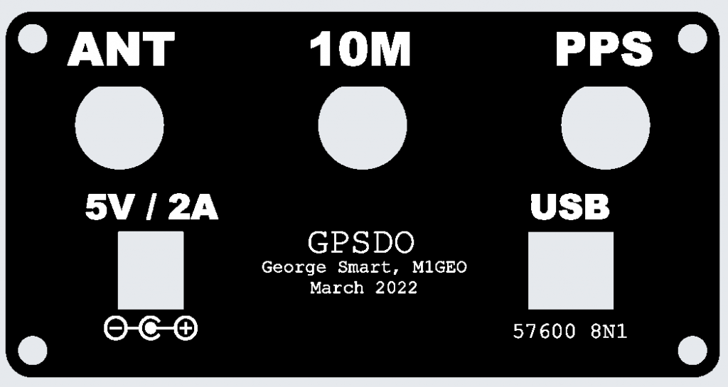
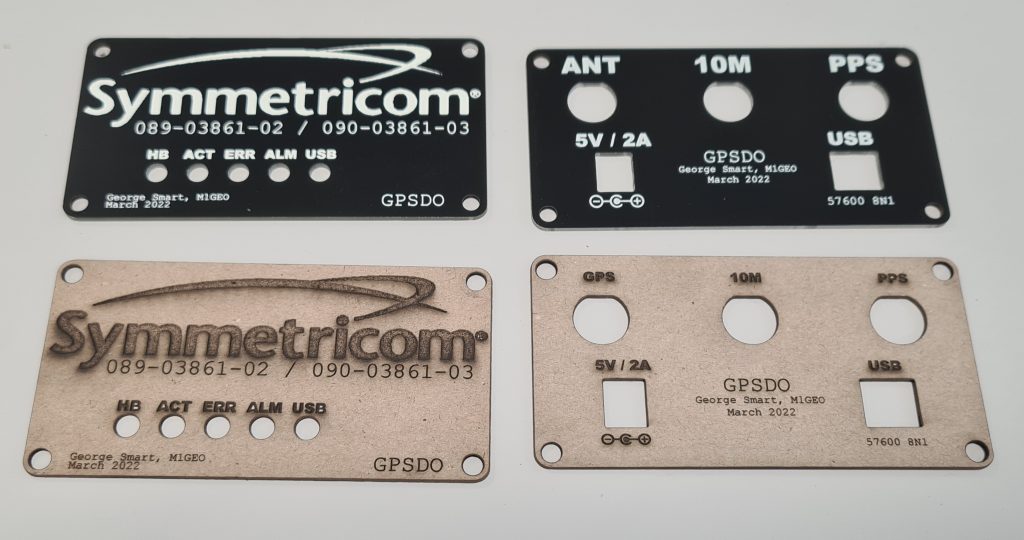
The project was designed to fit inside a Hammond Manufacturing 1455N1601BK case which takes a 160mm long by 100mm wide PCB, and the designed PCB fits the case nicely. By default, the Hammond case comes with either aluminum or plastic end plates, but I went to the effort to make PCB front and rear plates to enclose the case. Using PCB meant I was able to use tools I was familiar with to create the end places, and use the same order as the main carrier PCB. The copper on the PCB could be used to create a metal Faraday screen to enclose any electrical switching noise, and the silkscreen could be use to add legends, logos and decals.

I prototyped the designs as below in the PCB package and then used my laser cutter to test them out for fit. A test fit of the front panel is shown below:

The below picture shows the PCB end boards as they arrived and the cardboard cutouts. There are some small tweaks, between the two, but overall the process worked well. One thing to note is that the internal cutouts for the BNC connectors are a little bit tight – in future I need to add an extra 0.5mm or so clearance (in addition to the 0.5mm clearance I left already). However, the connectors pushed in even if a little tightly.

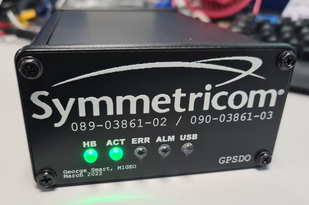
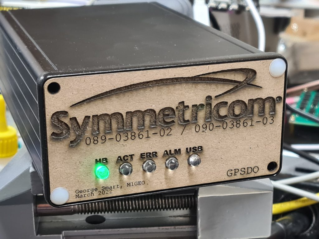
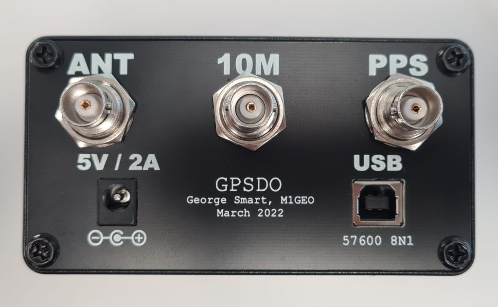
Final assembly went well, and I am very pleased with the results:

Erasing EPROMs in 2021

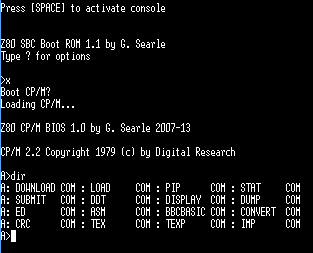
While chatting to a friend recently about an old Z80 CP/M machine I built based on Grant Searle’s Z80 CP/M machine, I decided to fire the machine up for a demonstration and give it a try.

No description available.

The machine had been in a shelf in my conservatory for well over a year since I last powered it, and when I connected the power, it was clear that there were signs of life, but, the machine was not happy at all! I could see bus conflicts on the data bus as well as very ‘broken’ behaviour.

After probing around, I decided to check a couple of logic gate (those controlling the address and read/write lines) using my TL866ii+ programmer which conveniently supports logic gate testing and RAM testing. All of the logic gate ICs confirmed to be working correctly, as did the 128Kx8 RAM chip. Checking the EPROM yield a different story!

Forgetful EPROM

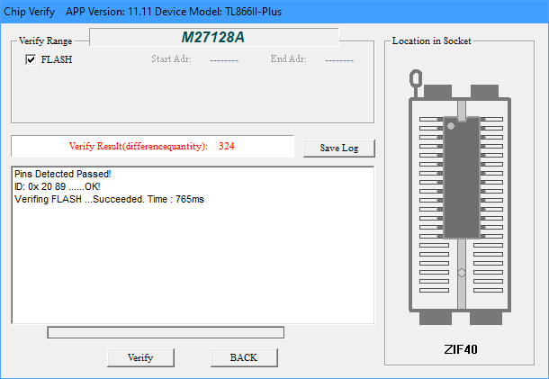
Some of the bits towards the end of the ERPOM had been erased (with UV erased parts, this means a ‘0’ bit had become a ‘1’ bit). The snapshot below shows in red bytes that had failed the verification.

The first 0x2012 bytes were completely unaffected with 324 differences in total (just under 2% of the 0x3FFF bytes in the 16KB ROM) mainly concentrated in the end of the address range.

This teaches me to always cover the UV window with something opaque as per the datasheet’s advice. I know people say that sunlight can erase such devices, I never really believed them. As an aside, others have looked into this, which I had not seen until now: see this hack-a-day article for a timelapse of EPROM data when exposed to sunlight.

And, secondly, it left me in a quandary as to how I should restore the ROM code.

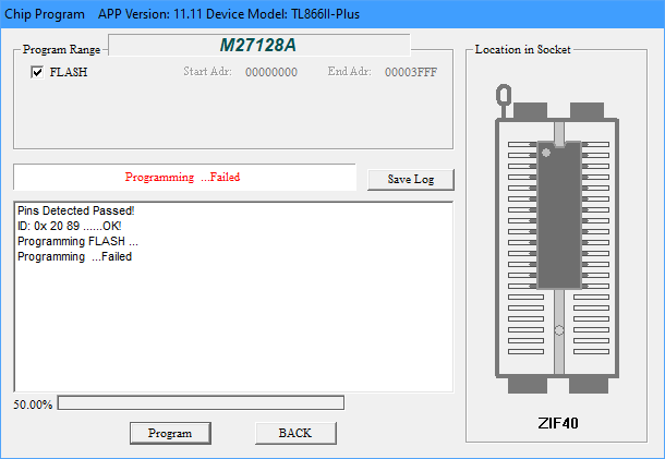
Initially I thought I should just be able to reprogram the device over the top of the existing code, since the changed bits would be reprogrammed back to ‘0”s from their current ‘1’ state. But, this turned out not to work. I’m not sure why, but the programmer would fail at 50% – just about the time the corrupt bits arrived.

I decided the next thing to do was to try and erase the IC – but how!?

Erasing UV EPROMs

I didn’t have one of the classic EPROM eraser boxes with a timer and a nice antistatic mat. I’d have to improvise. Essentially tinker around until the PROM was erased (reading 0xFF in all locations).

Eprom Eraser UV141 Professional made by Industrial electronics Ltd. UK

My first attempt was with a DSLR camera flash. I had seen these cheap EPROM erasers online that look like a xenon flash tube, so figured it was worth a shot. However it made no difference at all – I assume the camera flash has an UV filter.

My second attempt was with a UV LED, inspired Charles Ouweland‘s investigations along similar lines. Charles reports that this took 48 hours to erase the PROM. Like always, I was in a rush, so this didn’t really work for me. I could have driven a roundtrip to my parents (Dad has a proper UV eraser) in less then 4 hours including a cup of tea and a chat with Mum!

The third attempt was to use a UV insect-o-cutor which features UV fluorescent tubes as in the UV141 eraser pictured above. I placed the chip on the desk mat and put the UV insect-o-cutor directly on top such that the finger guard was on the top of the IC and the bars were not obscuring the window.

The scary part of this was that the high voltage aspect of the bug-zapper was popping on occasion with small insects – thankfully, the insects popping did not obscure the IC window nor cause ESD damage! After 20 minutes (the usual time I run the UV141 for) the IC was exactly the same. No additional bits had be cleared to logic ‘1’s. I suspect the output is UV-A and not the required UV-C.

Making a UV-C EPROM Eraser

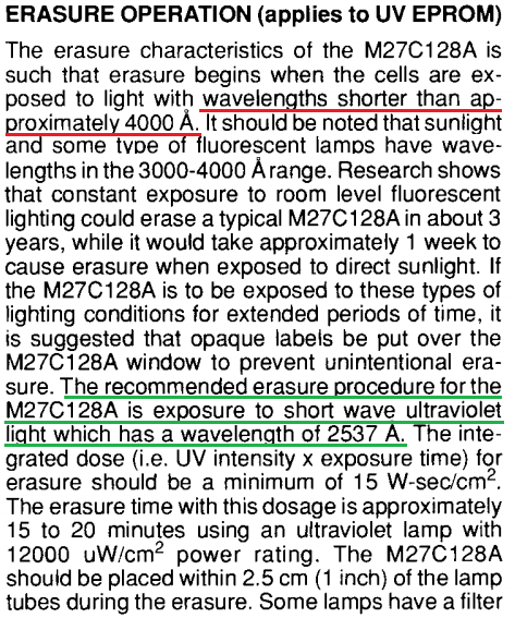
I went back to the second approach with the LED, this time consulting the EPROM datasheet (extract below), and noted that the recommended wavelength for erasure is 2537Å (253.7nm). This puts the UV light required to erase the EPROM in the UV-C spectrum.

I set about trying to find an LED with the correct wavelength. Some more digging showed up the VLMU35CB20-275-120 UV-C (270-280nm peak) LED offering a typical 13.5mW. Such wavelengths are common for curing acrylic nails and for sterilising surfaces in medical applications. At the time of writing, one such LED costs around £4.50 with VAT.

Constant LED Current

These LEDs appear to require between 5.0 and 7.5V at 120mA. I opted to create a simple constant current device using an LM317 set to 120mA and the two LEDs in series. This should work fine when supplied with at least 18V (7.5V + 7.5V + 3V [LM317 dropout voltage]). A SOIC8 LM317 is capable of 200mA and low profile enough to allow the LEDs to be close to the EPROM without catching. R1 is chosen to cause a voltage drop of 1.25V (the LM317 reference voltage) at the desired current. See this TI flashback for more details.

R1 = 1.25V/I = 1.25/120mA = 1.25/120e-3 = 10.4Ω. The closest easily available value is 10Ω, which checking backwards would give a current of 125mA. Since the datasheet mentions 150mA supply giving increased power, I have chosen to go with 10Ω as this will not damage the LED.

We should also consider the size of R1. The power dissipated in the resistor is easily calculated:

P = I^2 x R = (125mA)^2 x 10Ω = 120e-3^2 x 10 = 0.144W = 144mW.

So, a standard ¼-Watt through-hole resistor would be fine. For surface mount, 0805 resistors are typically 100mW, so a combination of multiple resistors should be used to handle the power. This could be four 10Ω parts in series-parallel, two 22Ω resistors in parallel (making 11Ω [114mA in the LEDs]), or two 4.7Ω resistors in parallel (making 9.4Ω [133mA in the LEDs]). I’ll opt for two 4.7Ω resistors since this is still below the maximum recommended working current of 150mA.

Designing the PCB

Initially I had considered tacking two wires on the LED and using a lab power supply to power the LEDs. However, I figured if I was making a constant current supply – mainly to avoid a “oops!” moment and pop £8 worth of LEDs – I would make a PCB to house it all. This way, I could keep the board with the EPROM programmer in the programmer box. The design brief would be simple. The PCB should fit inside the EPROM programmer (TL866ii+) box. The PCB should be (maximally) 110x50mm. I figured 100x50mm would be a nice size. A 5.5×2.1mm DC jack would allow for easy connection to wall-wart PSU or other power source. The rest was just two LEDs, and LM317, two resistors and a decoupling capacitor or two!

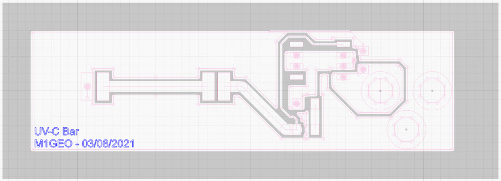
Since the PCB is quite simple, I figured it would be a good candidate to make with a laser cutter. Above shows an overlay of the Gerber edges and the layer to be etched. The back areas are there copper is to be removed. The white areas will remain copper.

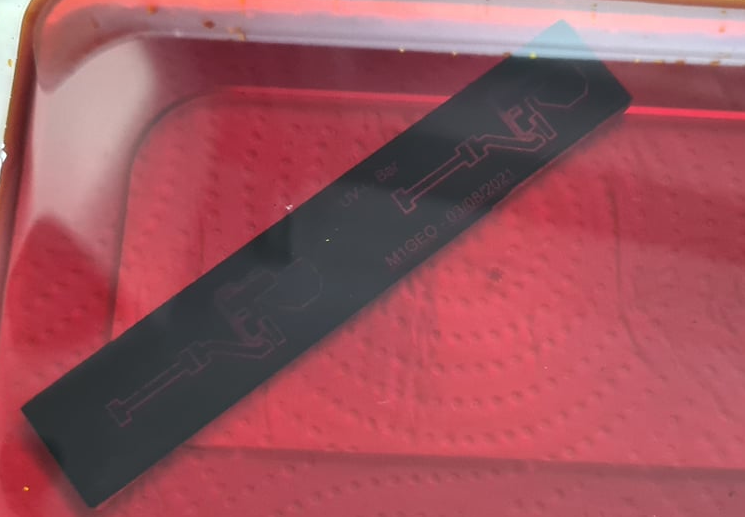
The board was created by coating a standard single-sided FR1 copper PCB blank with black paint from an aerosol can. This will be used as the etchant mask. The laser cutter is then able to remove the mask by burning away the paint layer, exposing the copper to the etchant.

No description available.

Typically, I’d also cut a solder mask from mica sheet to help apply paste, but for such a simple board, it isn’t worth the extra effort and waste materials.

The next job is to etch the PCB in ferric chloride – you should strive to make a much better job than I did!

I completely over-etched by board by having the etchant too cold and leaving it far too long! But hey, it’s been 10 years since I last made a PCB in my (parents) kitchen sink!

No description available.

From the image above you can see that my 10 thou track has completely disappeared in the right etch, and has almost completely disappeared in the left. I then proceeded to make a mess of drilling the connector holes, misreading a 4mm drill as a 2 mm. The board ended up as a total mess, but, I got it working!

No description available.

My apologies for making such a mess of the board. However, as you can see, the two LEDs are lit and a current of 117.3 mA flows through the series LEDs. I may tweak the resistor values to get an extra 10mA or so, but for now, the result is good enough!

So, now to erase the EPROM

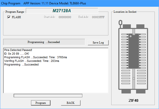
With the PCB made up, I eagerly put the EPROM back into the reader and loaded the old ROM code in. I reverified it to see that indeed 324 mismatches showed up, just as before. Confirmation that all my previous attempts had failed!

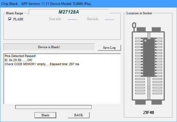
I held the newly made PCB above the UV window and gave the EPROM a 1 minute ‘blast’. I read the EPROM again, curious to see how many extra bytes failed verification. Too my surprise, 1088 byte failed verification – considerably more than before. I looked through the data and could see a pattern; the EPROM was blank. Sure enough, the 1 minute blast was enough to clear the EPROM!

I guess it just goes to show what having the right tools for the job can do!

Now will the computer boot?

Since I was on a roll, I reprogrammed the EPROM with the Z80 CP/M code and went for a test boot.

And we’re back to life! This is a machine based on Grant Searle’s Z80 CP/M machine.

Laser engraving metal using zinc spray

While looking for a way to create front panels and detailing on homebrew equipment, I was pointed to a YouTube video by Mark Presling entitled Metal Finishing With Mark – Metal Engraving 101.

In the video, Mark explains how cold galvanizing zinc spray, when ‘excited’ by a laser, burns at a high temperature to permanently mark the surface of the material onto which the zinc was sprayed. Mark suggests that this only works on stainless steel, however, other videos show how it can be used on ceramics, glass and similar substrates to burn or melt the substrate. I’m not exactly sure of the process, but, it certainly does leave a controllable, visible mark on the surface, which is exactly what I was after!

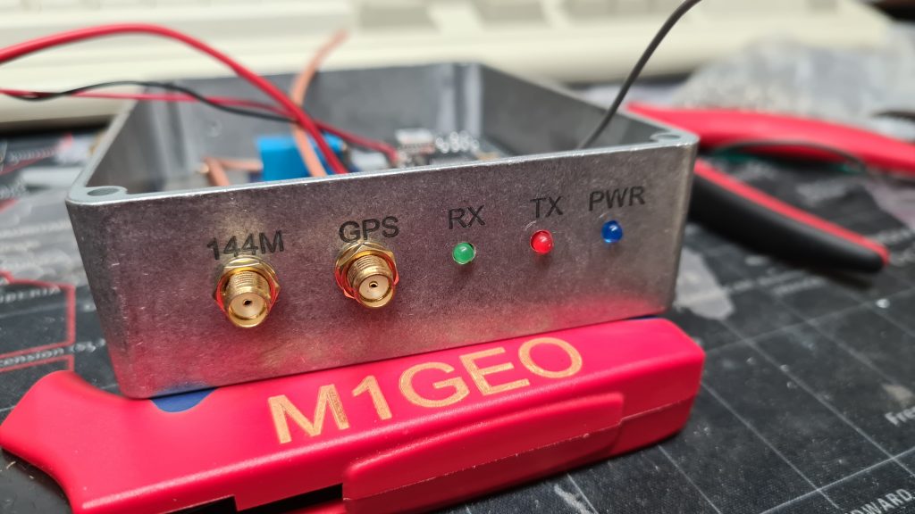
The box above shows markings for the 144 MHz antenna, GPS antenna, and status LEDs for an APRS transmitter I happened to be working on at the time. The effect is to leave a darker surface on the Hammond diecast box, which (at least to my testing) is very hard wearing and does not come off with use of solvents…

Here’s how

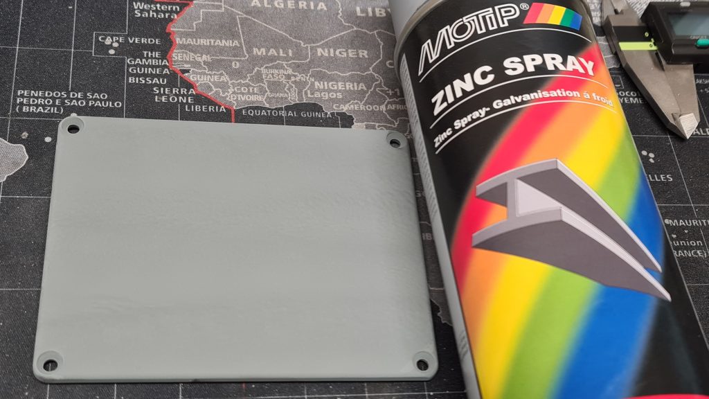
Firstly you’ll need to coat the surface to be etched with a liberal spray of zinc cold galvanizing compound. I used MOTIP Zinc Spray because it was the cheapest I could find on eBay and it works just fine – perhaps I got lucky but I’ve seen several videos on YouTube each swearing by a different make of spray, and they all appear to work. The important thing is that it is high in zinc. It’s an epoxy based aerosol, so, spray outside using the appropriate precautions. The spray should be quite thick, I spray on about 4 heavy coats one over the other and then let it ‘dry’ for around 5 minutes, just until the main solvent has evaporated.

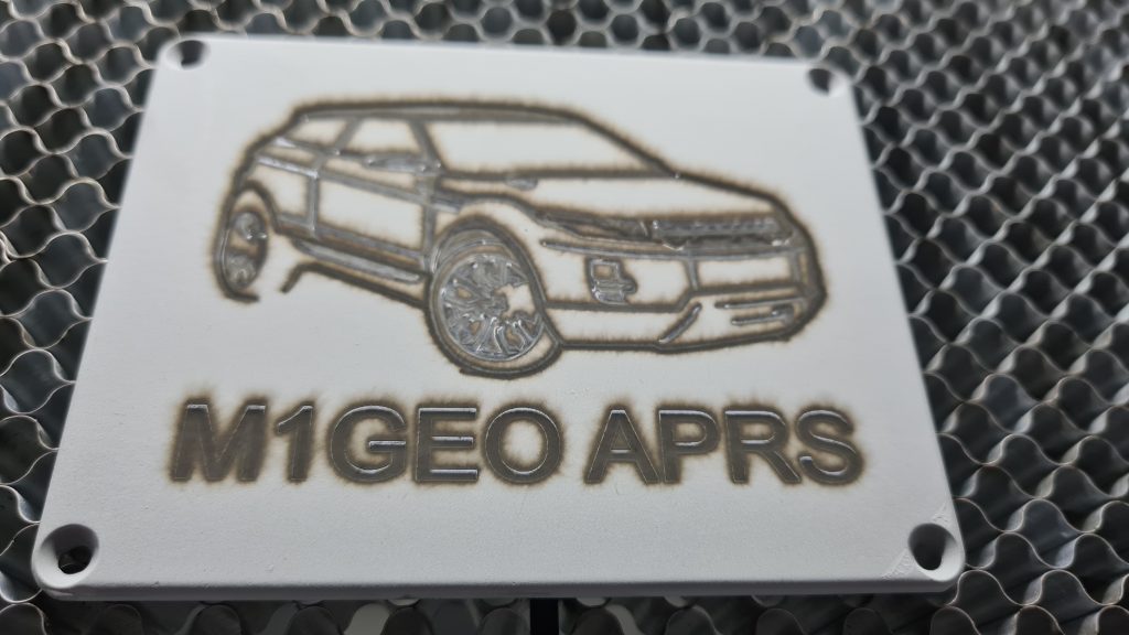
While the spray is drying, design your artwork. I’m making a line drawing of the car along with my callsign to put on the box, mainly to see how it comes out – I’m keen to see if the line drawing comes out well or not – so watch this space! My design looks like the following:

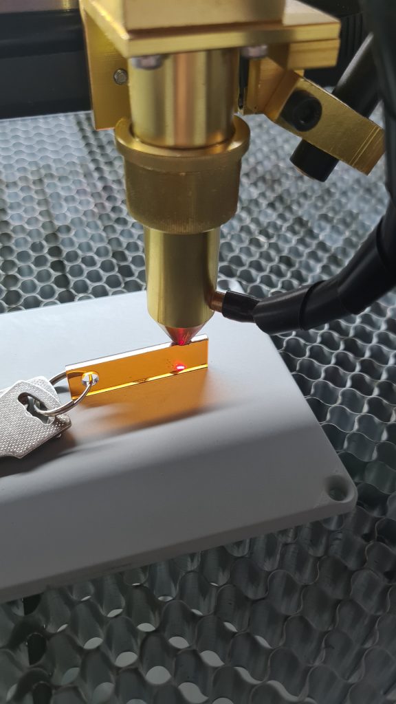
Next we get to put the metal into the laser cutter. I use a 60W CO2 laser cutter, with the power set to around 50%. Others have reported success using 10W diode lasers. I found that 50% was about right for my machine. Going slowly helped a lot, I reduced the machine to around 5mm/second. Where possible, vector engrave as the laser power is continuous and more controlled than raster scanning, but for large areas, such as the text, raster scanning works fine. I always reinforce text with a vector engrave around the outer.

You’ll need to focus the machine as you’d normally do in order to cut the surface.

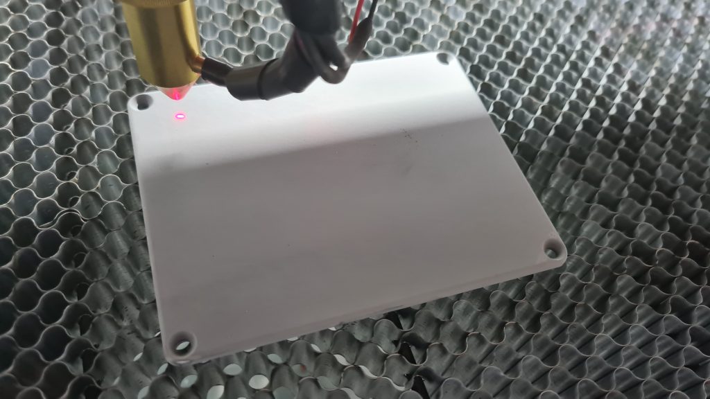
Once focused, frame the metal on the cutter bed. My laser cutter has a spotting laser which really helps with this.

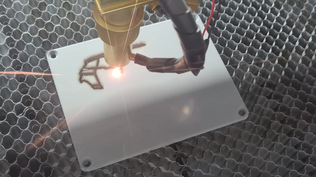
At this point, you’re ready to go! When the paint is hit with the laser, it goes a very burnt/sooty black. The process generates some very nasty fumes, which you are well advised not to breath – this includes metal vapors which are incredibly dangerous.

Once the engraving is done, leave the work in the cutter’s fume extraction for a short while to be sure that the chamber is clear of toxics, and then remove the work. Mine looks like this:

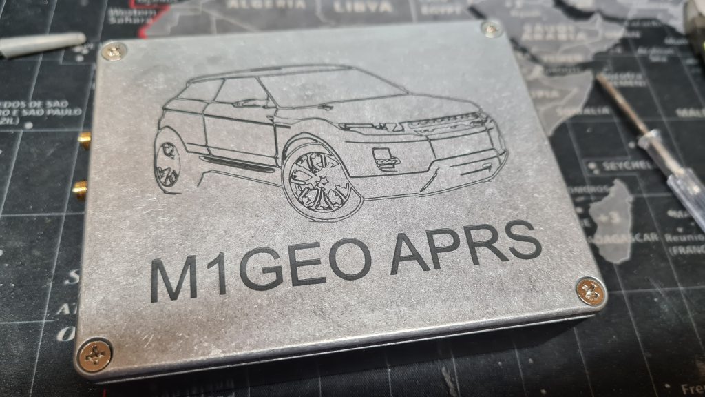
The final stage in the process is to use a paint remover to remove the paint from the metal to reveal the final design. I use cellulose thinners, which works well. Be sure to do this in a well ventilated space, otherwise you end up with a headache (like I have now, as I write this!).

I think you’ll agree that the final result looks very clean and tidy, and has retained all of the detail present in the original design.

This process is quick and easy to do if you have a laser cutter, uses a cheap-ish (around £6) can of zinc spray, and produces good, repeatable results with minimal fuss. It’s very useful for creating front panels and similar.

You may also find that spraying another colour of paint over the top, and then sanding down very lightly will further accentuate the design.

Characterising some VCOs for use in a GPSDO PLL

A key part of a GPS disciplined oscillator is the oscillator itself. During earlier testing I had used two Trimble 34310-T2 OCXO units and one seemed to perform much better than the other. I later read that this may be due to their aging, and that they gradually drift away from their optimal frequency – in this case, 10.000000 MHz – which in turn makes the phase-locked loop (PLL) struggle to converge the frequencies (and thus phase) of the loop. I also have a couple of IsoTemp 143-141 OCXOs, which I will measure, too.

The PLL compares the incoming phase of a reference frequency (here, derived from GPS timings) and the oscillator we’re ‘disciplining’. The loop can work in many ways, but, a common technique is to use digital signals from a phase-frequency detector though an analogue loop filter to generate some kind of voltage control voltage. This voltage is then fed back to the control pin of the oscillator, and the frequency changes accordingly. My post on using a Lattice FPGA development board to create a phase-frequency detector can be found in my Experiments with Phase-Frequency Detectors post.

My first task was to characterise the relationship between frequency and control voltage. For this task, I used a networked spectrum analyser in frequency counter mode and power supply, writing a simple Python3 script to twiddle the control voltage and record the corresponding frequency. I settled on taking an average of 5 readings at each voltage, with the control voltage swept at 100mV intervals through the specified VCO range. I repeated this for each of the oscillators I was hoping to use.

The IsoTemp 143-141 units have a much wider tuning range when compared to the Trimble 34310-T2 modules. In practice this means that the Trimble devices will have greater frequency resolution since they cover a smaller tuning range for the same control voltage range.

Another practical aside is that the IsoTemp 143-141 is a single-ovened oscillator whereas the Trimble 34310-T2 is a double-ovened module. This means that the Trimble unit is much less prone to external thermal variation. However, the IsoTemp unit as a larger tuning range, which will help the PLL keep in lock when there are large temperature variations.

The nominal 10 MHz frequency is found at the following tune voltage for each unit:

OCXO UnitApprox. Tuning Voltage (V)Measured Frequency (Hz)
34310-T2 Old1.9010000000.03
34310-T2 New3.7010000000.04
143-141 #12.1010000000.18
143-141 #22.009999999.78

It is clear from this that “34310-T2 New” is skewed to a higher voltage than the older Trimble unit.

I also observed the warmup time for each of the oscillator modules and the frequency of oscillation without any control voltage applied. Each unit was correctly orientated, supplied with the correct supply voltage as per the datasheet , and without any extra thermal insulation. The room temperature was 21C.

OCXO UnitApproximate Oven Warmup Time (m)Power Requirements (W)Natural Frequency (Hz)
34310-T2 Old~4 (sharp cut off)Max: 8.60
Norm: 2.08
10000000.88
(ΔF: 0.88 Hz)
34310-T2 New~4 (sharp cut off)Max: 8.62
Norm: 2.00
9999996.80
(ΔF: -3.20 Hz)
143-141 #1~5 (more gradual)Max: 2.63
Norm: 1.03
9999999.01
(ΔF: -0.99 Hz)
143-141 #2~5(more gradual)Max: 2.61
Norm: 1.10
9999999.87
(ΔF: -0.13 Hz)

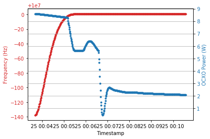
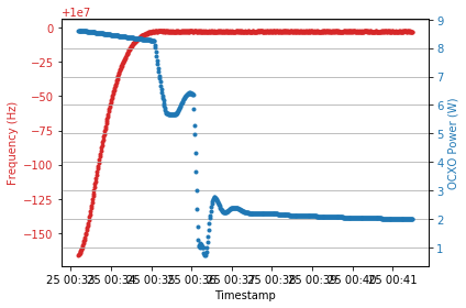
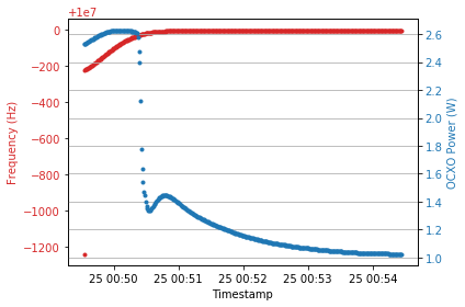
An example of the data captured during the warmup is given below for the Trimble units below:

34310-T2 Old:

34310-T2 New

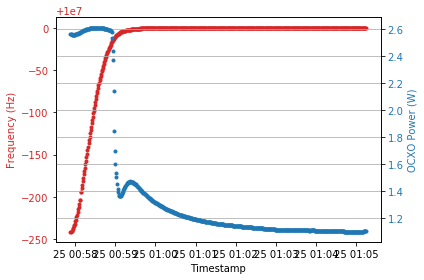
It is clear to see both Trimble units behave similarly, taking a similar time to warm up at around 4 minutes. The same data was obtained for both IsoTemp modules:

143-141 #1 – I suspect the first point at -1250 Hz is caused by measurement error and can be disregarded. This brings the unit inline with how #2 (below) responds

143-141 #2

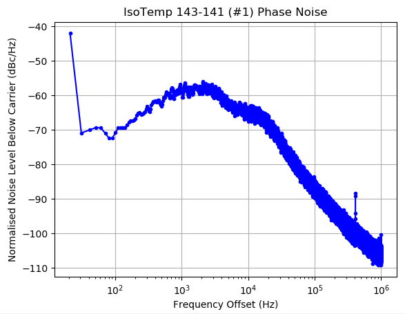
The next thing I would like to measure is the phase noise of both of the oscillator units. I have been playing around with scripting the measurement of phase noise of a signal using a spectrum analyser in clever ways. I am able to produce the following graphs. It is important to note that these graphs are not accurate!

A snippet from the IsoTemp 143 datasheet shows these measurements to be considerably distant from the expected results – again confirmation that the above graphs are not accurate.

For now, these are the best I am capable of producing. The numerical values are not absolute, although they should be comparable to those measured on a real noise analyser. However, they’re valid for an optician style “better-or-worse” comparison. I think it is fair to draw the conclusion that the phase noise of the Trimble unit is “better” than that of the IsoTemp unit. It is also worth noting that the output from the IsoTemp unit measured +13.5dBm (square wave), whereas the Trimble unit output only +5.3dBm (sine wave). This extra power required a slightly higher minimum attenuation in order to keep the spectrum analyser happy.

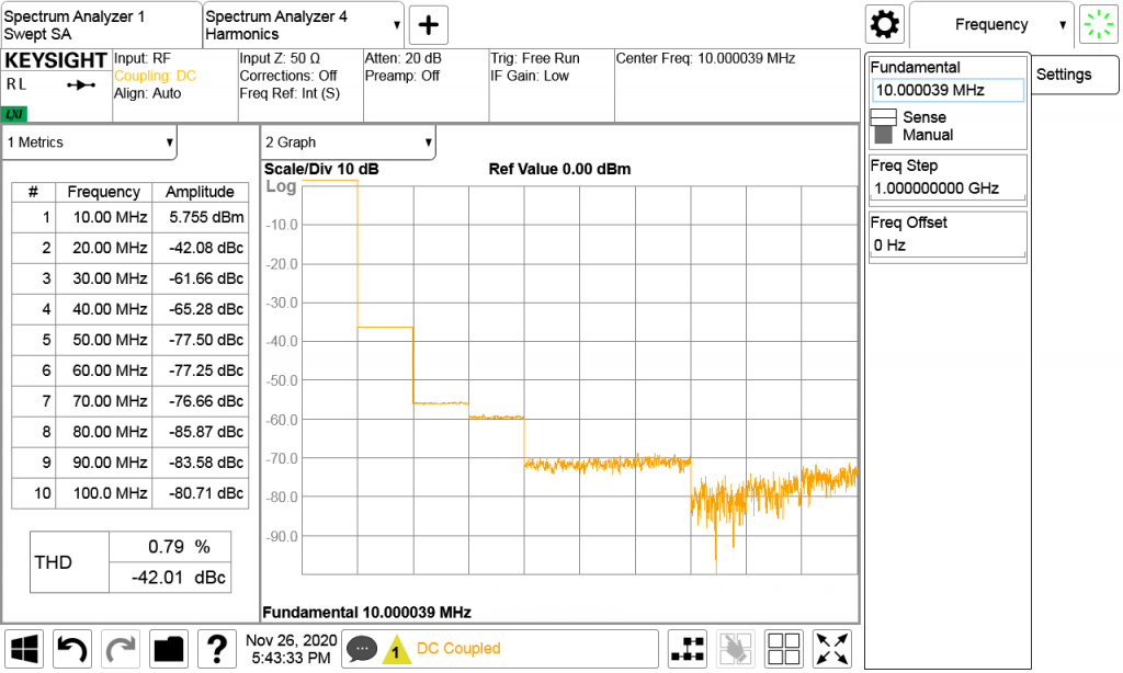
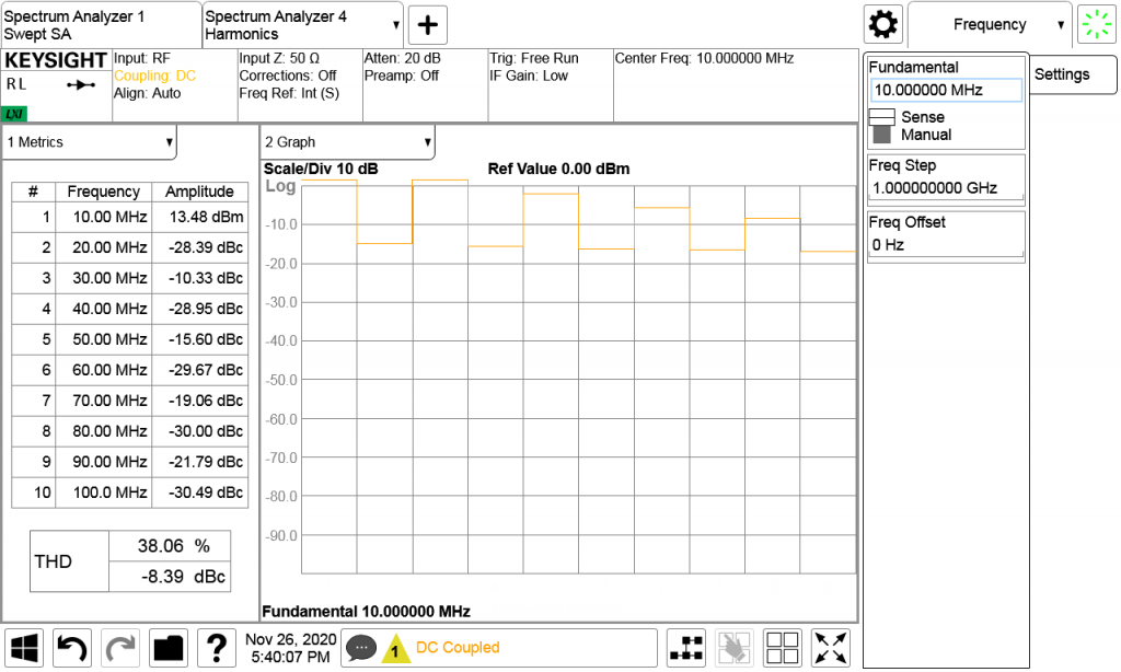
I also took the opportunity to look at the harmonic content for both types of oscillator. First the Trimble unit:

As expected, the IsoTemp produced high levels of odd-harmonics, which is to be expected given the square-wave output:

It seems that both the Trimble and IsoTemp parts are viable in the circuit I have been thinking of. The Trimble has a much more gentle Hz/Volt curve and as a result a smaller adjustment tolerance. Conversely the IsoTemp parts are considerably lower power (6W less, in fact, at peak), and also run at half the power (1W vs 2W) when at temperature.

180W PA Kit Construction

This page is about the Chinese RF_PA_250_3_HV_V201 by ZGJ 2018-01-25, version 201, commonly for sale on eBay, AliExpress, etc.

Sellers, you are welcome to link to this page in your listings.

This page is a mix of information from my own investigation as well as information found online (from several sources). It is useful for those purchasing kits for such amplifiers.

Bill of Materials

ReferenceQuantityPart
C1, C2, C8, C11, C19, C20, C21, C22, C24, C25, C261110nF (103)
C3, C9, C10, C13, C15, C16, C18, C468100nF (104)
R29110KΩ
R9, R10, R11, R1245.6Ω
C5, C122680pF Mica capacitor
C471100uF 25V
C7, C1421000uF 16V
L4, L52220uH Color ring inductance 
D91Red 2.54mm LED
D1019.1V Zener diode
(use with 24V power supply)
R301560Ω 3W
(use with 24V power supply) 
R7, R82220Ω 3W Power resistance
 120Ω 3W Power resistance
RV1, RV225KΩ or 10KΩ preset pot
L1113mm NXO100 magnetism ring (2 cores)
T1113×5 NXO magnetism ring
T21Copper pipe 2pcs, 0.75 square mm wire (60cm long), 18mm NXO magnetism rings (14 cores)
Q1, Q32IRFP250
U11LM78L06 or LM78L09
Insulating spacers2 
0.8mm enameled wire1 
0.75mm high temperature cable1 

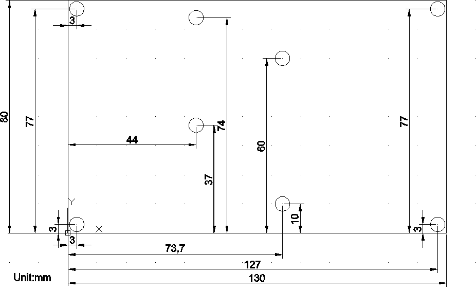
PCB Dimensions

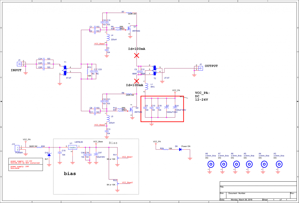
Schematic

Click image to enlarge. For transformer winding information, see below.

Build Information

Version History

  • V100 – First edition
  • V101 – Second edition: Output transformer cores reduced to 14.
  • V201 – Third edition: Power supply voltage is raised to 24V.

What you will need

  • 13.8V/24V 40A (or higher) power supply. It is better to have the function of current‐limiting protection. 6 square-mm (or more) wires for connecting the power to the amplifier board.
  • A signal source that is capable of outputting a 7 or 14 MHz signal at 10W.
  • A 50Ω dummy load rated for 200W (must be able to withstand continuous dissipation).
  • A heatsink suitable to dissipate the power of Q1 and Q3. (Recommended size: no less than 150x100x60mm).
  • A multi-meter that includes a 10A scale.
  • An oscilloscope capable of at least 20 MHz (or a spectrum analyser).

Before you start soldering

  • Wind the inductor (L1) and transformers (T1 and T2) in accordance with the information further on in this page.
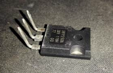
  • Bend the legs on Q1 and Q3 (TO247 package) upwards, see the illustration below. Do not mount it to the top side of the board. Do not shorten the leads.
  • Tap the holes for Q1 and Q3. Screw should be M3 (3mm screw). Clean the heatsink, and remove any metal chips to avoid a short circuit.

Soldering

  • Start with smaller components first, working up towards larger components and finally plugs.
  • SMT parts can be easily soldered with an iron by adding a small amount of solder to one pad, and using tweezers to push the SMT part into the molten solder on the pad. Once cooled, add a small amount of solder to the other pads.
  • L1 and C5/C12 are not fitted at this stage.

Preparation for Powering

  • Check for any solder splashes, and poor or missing solder joints.
  • Check the DC power supply resistance to ground – no short circuits. If you have not fitted L1 yet, test from the other side of L1 pad.
(Note: in the V201 version, there are 14 cores in the output transformer, not 16 as shown here)
  • Check the LM78L06 regulator output resistance to ground – no short circuits.
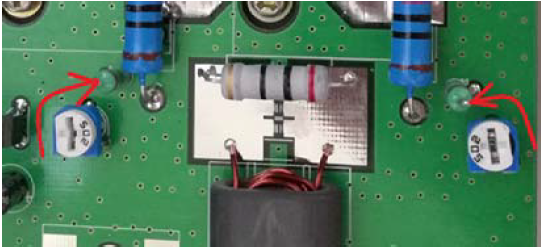
  • Check the bias-set variable resistors. Rotate them as shown in the following diagram. Be careful, to rotate them to the correct end-stop. If you get this wrong, you will destroy the IRFP250N power MOSFETs. You are aiming for an initial bias voltage of 0V.
  • Mount the input transformer secondary load resistor (10Ω, 3W).
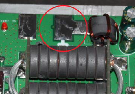
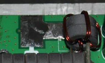
  • Solder in Q1 and Q3 and affix to the heatsink. Flow solder on the PCB trace between the MOSFET and the output transformer. This increases the current capacity of the track. See below.
  • Mount L1 as shown below.

Set bias currents

The aim of this section is to adjust the bias current to 100mA for each of the two transistors. When making adjustments, you must act slowly, and with great care – the current will do nothing for much of the adjustment range and then rise sharply. The transistors must be bolted to a heatsink during adjustment.

  • Double-check that the variable resistors are ‘zeroed’ as described above, such that when power is initially applied, there is no bias voltage present.
  • Connect a current meter in series with the positive power supply cable of the amplifier. Apply power.
  • Adjust the upper MOSFET quiescent (static) current using the upper variable resistor to cause an increase in current of 100mA (0.1A).
  • As before, now adjust the quiescent current of the lower MOSFET to further increase the current another 100mA. (A total increase of 200mA between both transistors.)
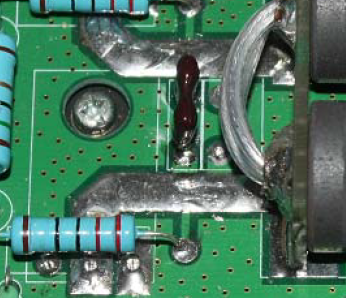
  • Solder in choke inductor L1 and mica capacitor C5/C12 if you have not already done so – the bias adjustment is complete.

Signal test

  • Connect a 50Ω dummy load to J2. The load must be capable of handling 200W.
  • Use an oscilloscope on a suitable range (or spectrum analyser with suitable attenuation) to monitor the signal at the load.
  • Connect the power supply and monitor the supply current for a moment. If the current is gradually increasing, the power must be cut immediately and check for suitable thermal connection between the power transistors Q1 and Q3 and the heatsink.
  • With the amplifier powered and no input, check the oscilloscope for signals. If there signals, immediately power off and debug the cause of self oscillation.
  • Input a small signal, gradually increasing the input signal power.
  • Observe the output waveform and the DC input current. In general, 100Vpp output across the output load corresponds to a power output of 25W into 50Ω. A load voltage of 141Vpp is 50W output, 180Vpp load voltage gives an output power of 80W, and 200Vpp at the load is a power output of 100W. Using an efficiency of 55% as an approximation, the expected DC power input can be calculated.
  • Check the temperature of the heatsink. If it is too hot to hold, then you will need to use a fan to cool the amplifier.
  • Check the output power is stable over time, and that there are no large fluctuations in output power for a fixed input power.

Finishing

  • Use a flux remover to clean any solder flux residue and tidy any poor solder joints.
  • Mount the amplifier into a box or case with suitable TX/RX switching.
  • Accompany the amplifier with a suitable low-pass filter board.

Transformer & Coil Winding

In the following diagrams process, please note:

  • To avoid scraping the enamelled wire, use needle nose pliers to smooth the edge of the ferrites. Hole edges may be sharp.
  • A “turn” on the coil is regarded as wire passing through the centre.

Winding T1

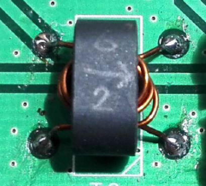
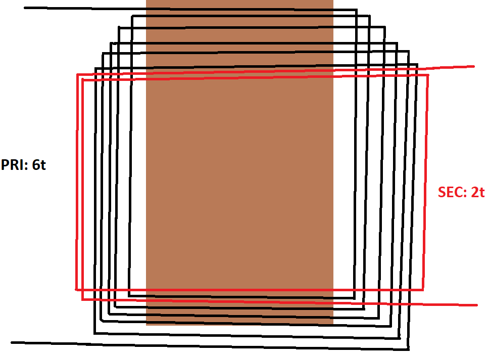
Transformer T1 primary should be 6 turns (black lines). The secondary of T1 should be 2 turns (red lines). The turns ratio is important, since if there are too many turns, the voltage on the gates of the MOSFETs will exceed the breakdown voltage and the parts will be destroyed.

Winding T2

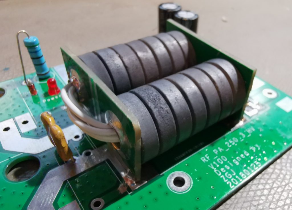
Transformer T2 primary should be 1 turn made from the two end PCBs and copper pipe. The secondary of T2 should be 5 turns of high temperature wire.

In version 201 of the kit, the number of ferrite rings is reduced from 16 to 14. You will also need 2 ferrites for winding L1 (see below).

Winding L1

L1 is a high frequency RFC choke. The 7-10 turns should be wound around two ferrite rings as used in T2. I chose 10 turns as this provides the largest choke inductance.

Experiments with Phase-Frequency Detectors

Over the past few evenings, I have been experimenting with phase-frequency detectors. I have an upcoming project that requires the use of one, and, I figured I’d refresh my memory on them. I ended up using my Lattice MachXO2 breakout board as the development platform.

The first step was to divide a 10 MHz crystal oscillator down to 10 kHz. That was easily done with a counter, counting from 0 to 499, and then resetting to 0. Every reset would simultaneously toggle an output bit, with the net result being a square-wave clock on the output bit, periodic every 1000 cycles of the input. A divide by 1000 counter.

Next was to understand the Phase-Frequency Detector (PFD). This is commonly referred to as a Type 2 detector, since it detects not only phase difference but frequency difference. This means that the PLL will only ever lock to the fundamental frequency, and not harmonics. It also means that when the loop is unlocked, the PFD knows which way to drive the VCO to regain lock. A Type 1 detector only uses phase information, and so drives the oscillator in the direction of the phase difference until the loop locks – as a result, Type 2 detectors lock quicker.

The Type 2 detector has two outputs, up and down, which pulse for the required direction with a duty cycle proportional to the phase difference.

I spent a few days designing and simulating the PFD using the Aldec Active-HDL simulator to confirm that my circuit did indeed perform as expected:

I then added a simple lock detector, which set a locked signal high if the phases were in lock for the past 10 cycles as a proof of concept. In reality, a much longer observation window will be used. It is possible to see the lock signal becomes high after 10 cycles.

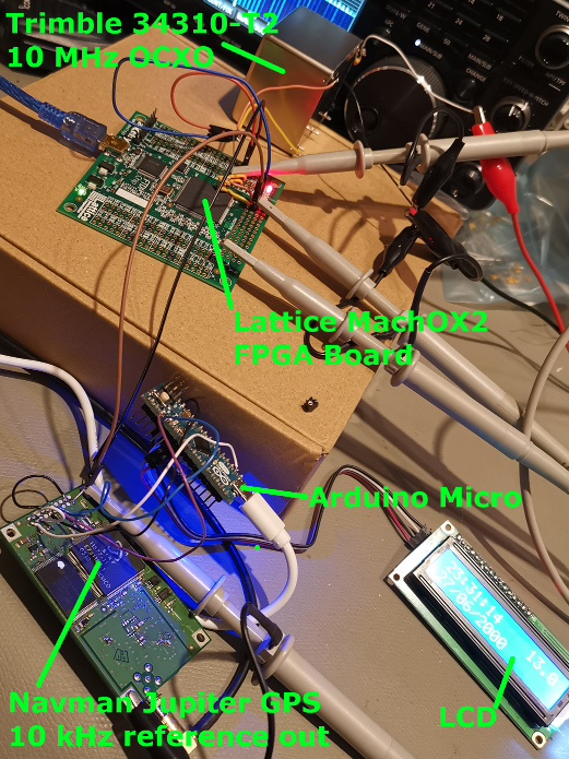
The final stage of this project snippet was to test on real hardware. The Verilog code was pushed through synthesis, place and route, and a configuration file for the Lattice FPGA generated. This was then programmed into the board, and the board taken to the lab – you can see all the main parts of the setup in the photo below.

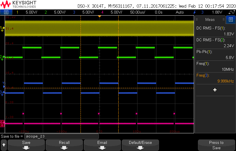
Below, you can see the scope traces from the probes in the lab bench photo. The yellow trace shows the 10 MHz VCO frequency from the Trimble 34310-T2 OCXO. The green trace is a debug from the FPGA output showing the 10 MHz signal divided down 10 kHz. The blue trace is GPS locked 10 kHz reference output. Finally, the purple is phase detector output, here from the ‘down’ output of the detector since we see that the divided VCO output (green) slightly leads the GPS reference (blue). The ‘up’ output is at logic-0 throughout.

The next part of the project was to create the charge pump circuit which converts the ‘up’ and ‘down’ pulsed signals into an analogue control voltage for the VCO.

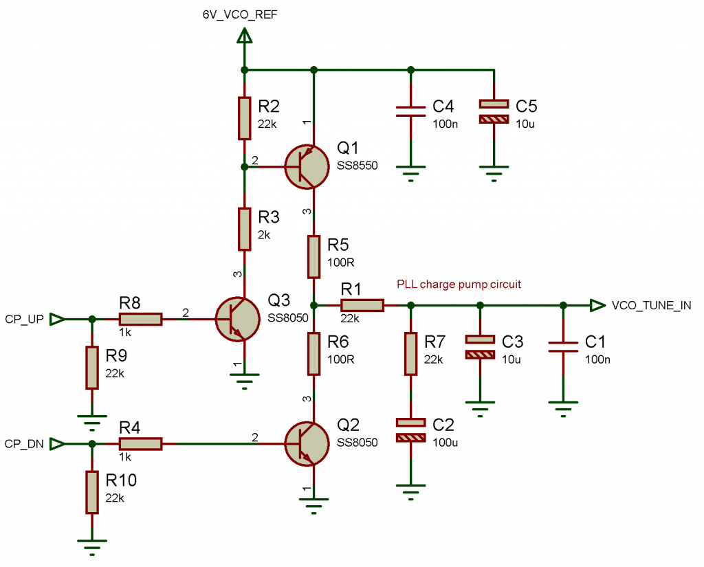
The parts for the charge pump took a few days to arrive, and while waiting I contrived the following circuit. Since the OCXO generates a 6V reference voltage for use with the VCO input (actually 5.4V in my case), it seemed wise to use that. Some crude experiments had lead me to a tune voltage of around 3.5V. The circuit uses a PNP transistor (Q1) to put pulses of energy into the filter network via R1. Similarly, it uses an NPN transistor (Q2) to remove pulses of energy from the filter via R1. R5 and R6 serve as a current limit in case both Q1 and Q2 are both powered. A further NPN transistor (Q3) acts as a voltage interface between the ~6V on the base of Q1 and the FPGA IO at 3V3 maximum. Only the values of components in the filter section are critical (R1, R7, C1, C2, C3); the others were chosen from what I had laying around.

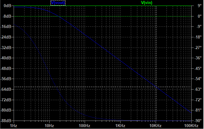
The loop filter was tested and tweaked in LTspice using the values above. The loop filter has around 62 dB of attenuation at 10 kHz (our reference [and thus up/down pulse] frequency).

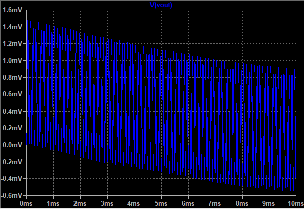
A look in the time domain shows we can expect about 1.5mVp-p at 10 kHz from visual estimation. An output of 1.5mVp-p is approximately 0.53 mVrms, which gives us around -66 dBV of attenuation (similar to we saw above). The curve of the waveform is the DC levels settling out at the start of the simulation.

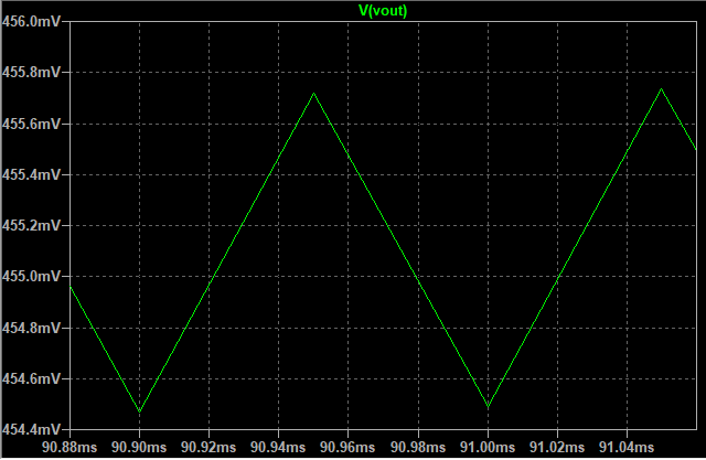
And finally the steady-state ripple; for a 1V square wave (0V-1V) input, a 1.23 mV ripple exists at the output (455.719-454.486).

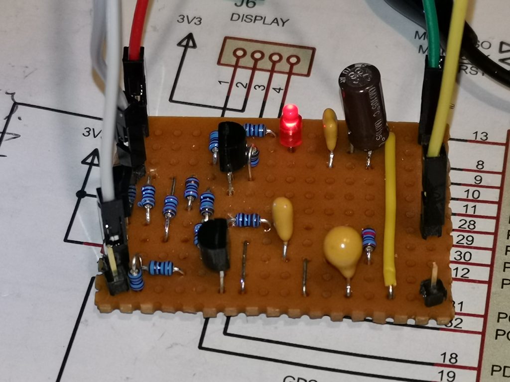
The penultimate step was to build the circuit and confirm it worked in real life. I made the charge pump on a scrap of strip-board, with pin headers for the main signals. On the left, +6V VCO reference input, the up and down signals from the FPGA, and on the right, ground and the VCO tuning input. The circuit is pretty much laid out as per the schematic, with the addition of an LED.

The final step was to watch the PLL lock on the scope! In the short video clip below, you can see the yellow trace is the 10 kHz reference frequency from the GPS. The green trace is the 10 MHz from the VCO. The blue trace is the 10 MHz divided down to 10 kHz. The purple trace is the VCO tune voltage – the output of the charge pump.

The closing remark is that this project was a learning exercise. The Verilog code & TB is presented here on GitHub and you’re invited to take a look.

Installing Eclipse IDE and PyDev onto Ubuntu 18.04

This page assumes some basic familiarity with Linux. It assumes a clean install of Ubuntu 18.04 and installs Eclipse Photon. I install the CPP version, but you’re free to choose when the option presents itself!

Update the OS

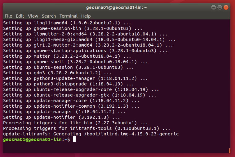
First thing to do is to update the operating system. This is easily achieved by running the following two commands:

sudo apt update

sudo apt upgrade

These commands may take a while to complete, depending on what there is to update and how fast your internet connection is.

Installing Java Development Kit (JDK) 8

Since Eclipse is written in Java, we will need the latest version. I’m not sure if the Java Runtime Environment (JRE) alone is enough, but I have installed the full JDK anyway.

Firstly we add the third party JDK PPA repository and update the package manger index

sudo add-apt-repository ppa:webupd8team/java

sudo apt update

Next we must actually install the JDK:

sudo apt install oracle-java8-installer

This will pull in a few extra packages, such as java-common, oracle-java8-set-default (which makes sure that this installed version of Java is the system default), font packages and so on. You’ll be guided through the Java 8 installation with an ncurses based installer:

You must accept the Oracle Binary Code licence. The download for Java 8-1u171 was 182 MB. To confirm the installer completed correctly, scroll up in the terminal window. You should see something explaining that the installation finished successfully. To confirm this, and check the version installed, you can run the following from the terminal:

javac -version

javac 1.8.0_171 [or similar result expected]

Installing Eclipse

The Eclipse installer can be found on the Eclipse project download page: https://www.eclipse.org/downloads/. At the time of writing, the Eclipse Photon installer was 45.9 MB. I downloaded it using the Mozilla Firefox browser, and saved the installer into my user’s download folder (/home/geosma01/Downloads/).

Once downloaded, switch back to your terminal program, and change directory into the downloads folder and extract the downloaded TAR/GZIP archive and change directory into it:

cd ~/Downloads/

tar xvfz eclipse-inst-linux64.tar.gz

We’re now ready to run the installer. If we change into the newly extracted folder and then run the installer, we should be good to go:

cd eclipse-installer

./eclipse-inst

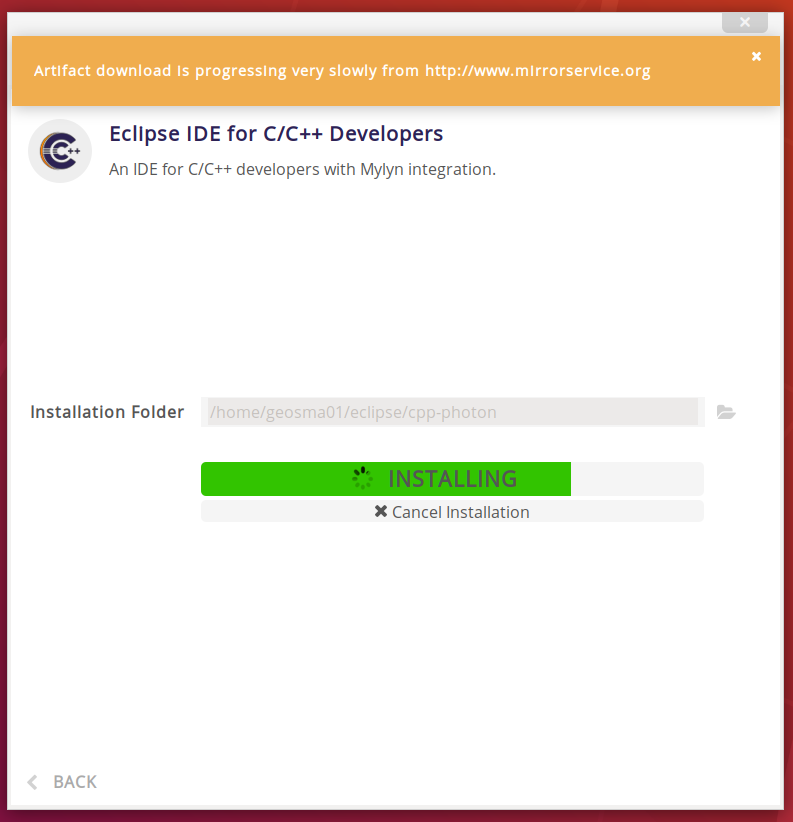
I ran into trouble installing Eclipse as root, so I install it into my own user space: ~/eclipse/cpp-photon

Accept any licences it prompts for:

Once the installer has finished, you can start Eclipse by pressing Launch. We’ll make a desktop shortcut in a few moments…

And eventually…

Now we have Eclipse running, we should get ourselves an icon to easily start it.

Creating a Menu Icon

Next we will create a menu shortcut. We will create this using a basic terminal-based text editor (nano). Running the following will open the file:

nano ~/.local/share/applications/eclipse.desktop

Then, copy and paste the following, as you see appropriate – you should change my username (geosma01) to your own at the very least:

[Desktop Entry]
Name=Eclipse CPP Photon
Type=Application
Exec=/home/geosma01/eclipse/cpp-photon/eclipse/eclipse
Terminal=false
Icon=/home/geosma01/eclipse/cpp-photon/eclipse/icon.xpm
Comment=Integrated Development Environment
NoDisplay=false
Categories=Development;IDE;
Name[en]=Eclipse

If all has gone well, you’ll see something like the following inside the menu:

Installing PyDev

PyDev can be easily installed through the Eclipse Marketplace. From inside Eclipse, click Help on the menu, and select Eclipse Marketplace. You should be presented with the following window. You can then enter “pydev” into the search, and then click Install on the entry shown below:

Confirm your selections, accept the licence conditions, and you’re good to go! Once installed, click on Restart Now and you’re done!

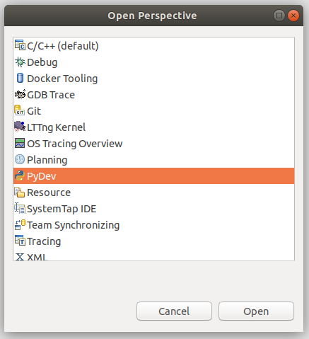
Once restarted, you can open a PyDev Perspective by selecting Window from the menu, selecting Perspective > Open Perspective > Other and selecting PyDev:

You’re ready to go!