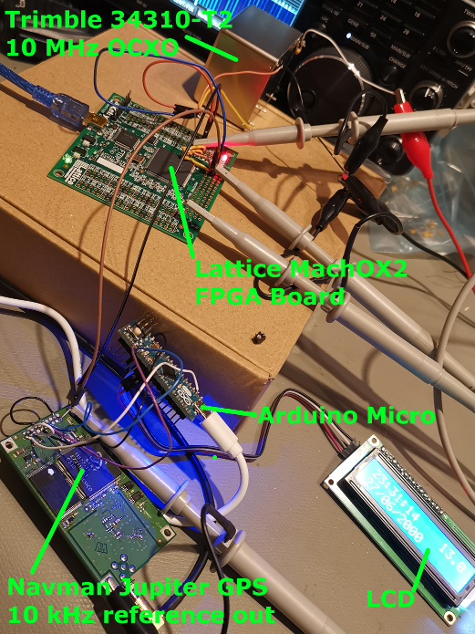
A key part of a GPS disciplined oscillator is the oscillator itself. During earlier testing I had used two Trimble 34310-T2 OCXO units and one seemed to perform much better than the other. I later read that this may be due to their aging, and that they gradually drift away from their optimal frequency – in this case, 10.000000 MHz – which in turn makes the phase-locked loop (PLL) struggle to converge the frequencies (and thus phase) of the loop. I also have a couple of IsoTemp 143-141 OCXOs, which I will measure, too.
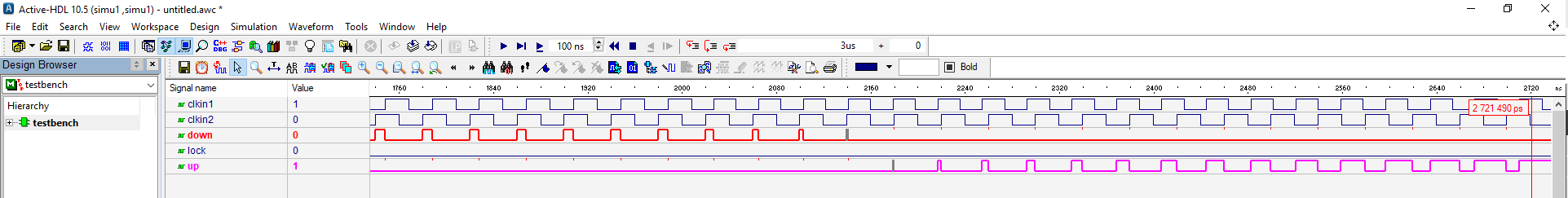
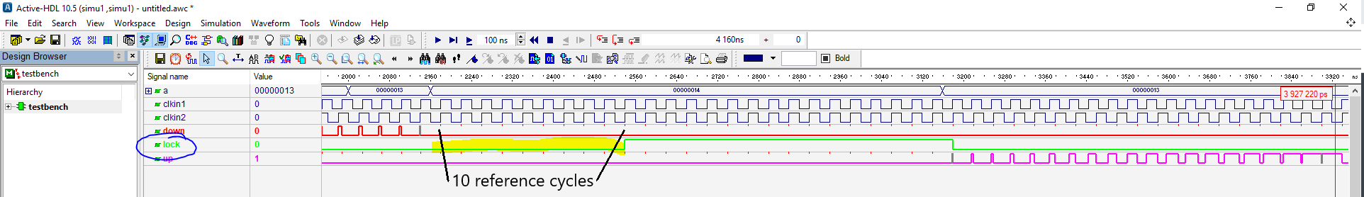
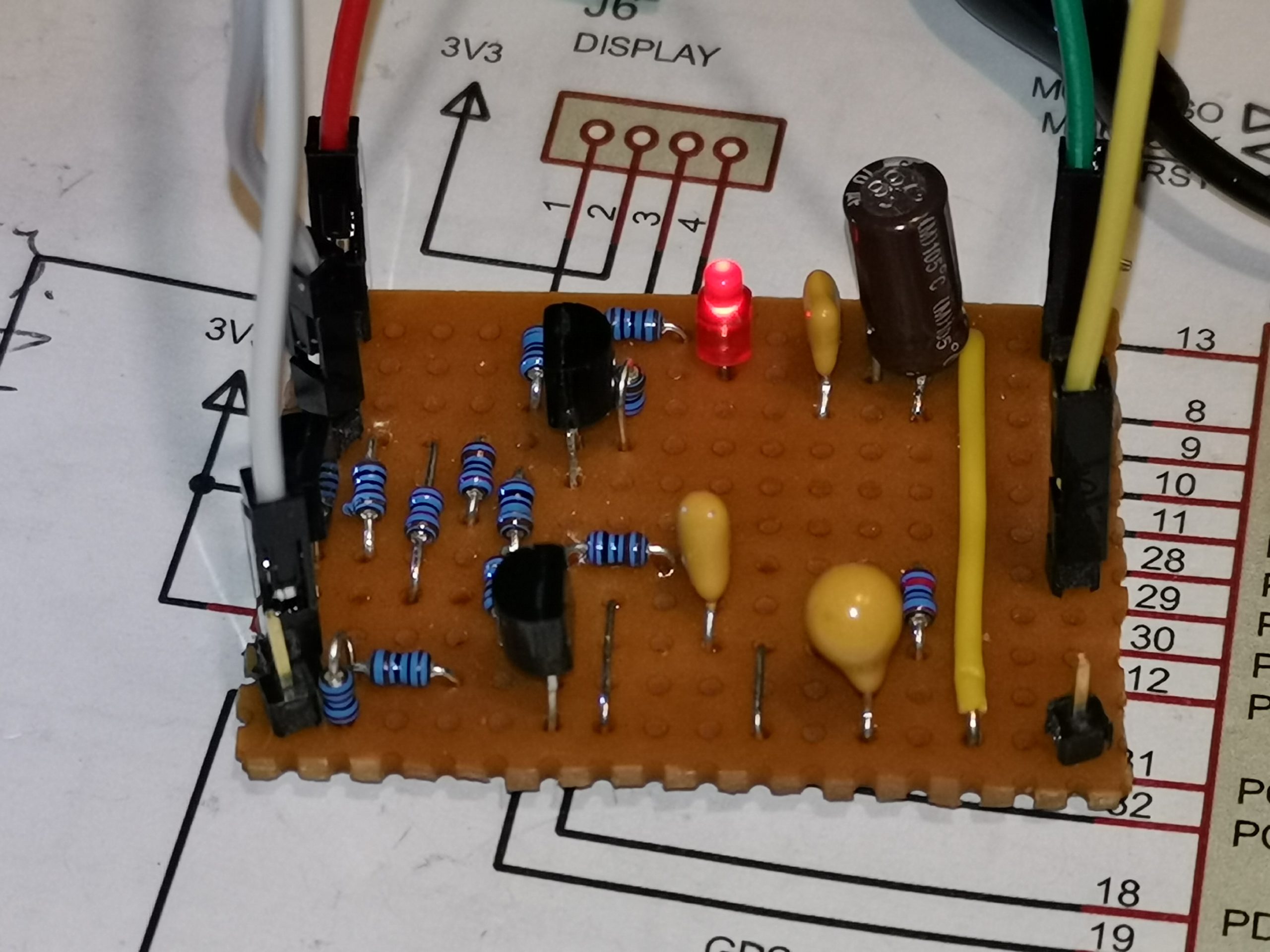
The PLL compares the incoming phase of a reference frequency (here, derived from GPS timings) and the oscillator we’re ‘disciplining’. The loop can work in many ways, but, a common technique is to use digital signals from a phase-frequency detector though an analogue loop filter to generate some kind of voltage control voltage. This voltage is then fed back to the control pin of the oscillator, and the frequency changes accordingly. My post on using a Lattice FPGA development board to create a phase-frequency detector can be found in my Experiments with Phase-Frequency Detectors post.
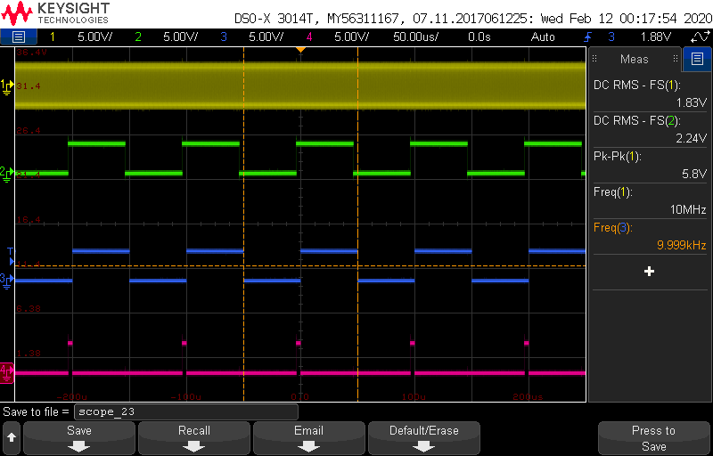
My first task was to characterise the relationship between frequency and control voltage. For this task, I used a networked spectrum analyser in frequency counter mode and power supply, writing a simple Python3 script to twiddle the control voltage and record the corresponding frequency. I settled on taking an average of 5 readings at each voltage, with the control voltage swept at 100mV intervals through the specified VCO range. I repeated this for each of the oscillators I was hoping to use.
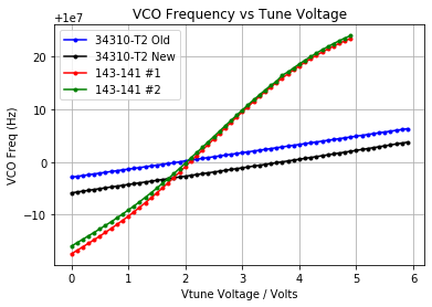
The IsoTemp 143-141 units have a much wider tuning range when compared to the Trimble 34310-T2 modules. In practice this means that the Trimble devices will have greater frequency resolution since they cover a smaller tuning range for the same control voltage range.
Another practical aside is that the IsoTemp 143-141 is a single-ovened oscillator whereas the Trimble 34310-T2 is a double-ovened module. This means that the Trimble unit is much less prone to external thermal variation. However, the IsoTemp unit as a larger tuning range, which will help the PLL keep in lock when there are large temperature variations.
The nominal 10 MHz frequency is found at the following tune voltage for each unit:
| OCXO Unit | Approx. Tuning Voltage (V) | Measured Frequency (Hz) |
| 34310-T2 Old | 1.90 | 10000000.03 |
| 34310-T2 New | 3.70 | 10000000.04 |
| 143-141 #1 | 2.10 | 10000000.18 |
| 143-141 #2 | 2.00 | 9999999.78 |
It is clear from this that “34310-T2 New” is skewed to a higher voltage than the older Trimble unit.
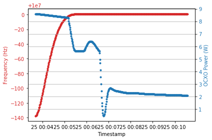
I also observed the warmup time for each of the oscillator modules and the frequency of oscillation without any control voltage applied. Each unit was correctly orientated, supplied with the correct supply voltage as per the datasheet , and without any extra thermal insulation. The room temperature was 21C.
| OCXO Unit | Approximate Oven Warmup Time (m) | Power Requirements (W) | Natural Frequency (Hz) |
| 34310-T2 Old | ~4 (sharp cut off) | Max: 8.60 Norm: 2.08 | 10000000.88 (ΔF: 0.88 Hz) |
| 34310-T2 New | ~4 (sharp cut off) | Max: 8.62 Norm: 2.00 | 9999996.80 (ΔF: -3.20 Hz) |
| 143-141 #1 | ~5 (more gradual) | Max: 2.63 Norm: 1.03 | 9999999.01 (ΔF: -0.99 Hz) |
| 143-141 #2 | ~5(more gradual) | Max: 2.61 Norm: 1.10 | 9999999.87 (ΔF: -0.13 Hz) |
An example of the data captured during the warmup is given below for the Trimble units below:
34310-T2 Old:
34310-T2 New
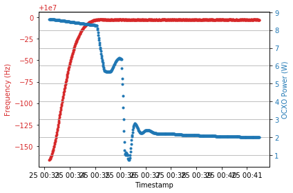
It is clear to see both Trimble units behave similarly, taking a similar time to warm up at around 4 minutes. The same data was obtained for both IsoTemp modules:
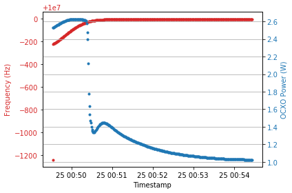
143-141 #1 – I suspect the first point at -1250 Hz is caused by measurement error and can be disregarded. This brings the unit inline with how #2 (below) responds
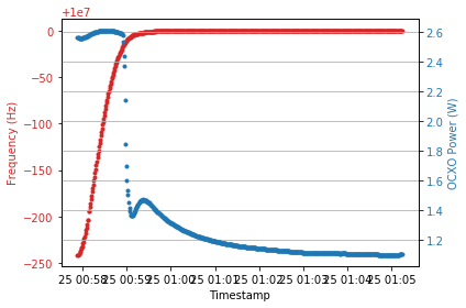
143-141 #2
The next thing I would like to measure is the phase noise of both of the oscillator units. I have been playing around with scripting the measurement of phase noise of a signal using a spectrum analyser in clever ways. I am able to produce the following graphs. It is important to note that these graphs are not accurate!

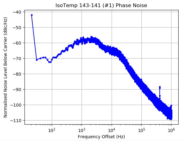
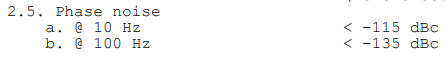
A snippet from the IsoTemp 143 datasheet shows these measurements to be considerably distant from the expected results – again confirmation that the above graphs are not accurate.
For now, these are the best I am capable of producing. The numerical values are not absolute, although they should be comparable to those measured on a real noise analyser. However, they’re valid for an optician style “better-or-worse” comparison. I think it is fair to draw the conclusion that the phase noise of the Trimble unit is “better” than that of the IsoTemp unit. It is also worth noting that the output from the IsoTemp unit measured +13.5dBm (square wave), whereas the Trimble unit output only +5.3dBm (sine wave). This extra power required a slightly higher minimum attenuation in order to keep the spectrum analyser happy.
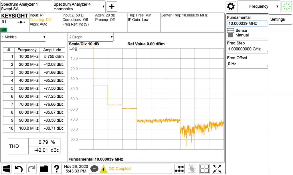
I also took the opportunity to look at the harmonic content for both types of oscillator. First the Trimble unit:
As expected, the IsoTemp produced high levels of odd-harmonics, which is to be expected given the square-wave output:
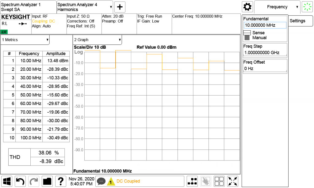
It seems that both the Trimble and IsoTemp parts are viable in the circuit I have been thinking of. The Trimble has a much more gentle Hz/Volt curve and as a result a smaller adjustment tolerance. Conversely the IsoTemp parts are considerably lower power (6W less, in fact, at peak), and also run at half the power (1W vs 2W) when at temperature.