
Exciter
The exciter board is based on my Arduino WSPR exciter. I do plan to create a better stand-alone board soon, with one of these Chinese DDS modules that are cheap and easy to get from eBay. At the minute I am using a DDS60 by AmQRP.
The output from this amplifier is small (around 980mV unloaded, about 290mV into  ). The scope trace below shows what the DDS-60’s output looks at 472 kHz. The sinewaves are a little flat-topped but this doesn’t matter as it’s only at the driver stage. The PA will be class-E and so will completely distort the signal and require cleaning later.

Visit this page for help getting this far.
Power Amplifier
Attempt 1
My first power amplifier was closely based on GW3UEP’s 25W PA. I adjusted some of the coil inductances and altered the design fractionally to better suit what I had, but it is still in essence GW3UEP’s design.
From the input waveform above, I have used a CMOS 4069 with one of the input gates biased half on to convert the input into a square wave to drive the FET. I used a very crude circuit:
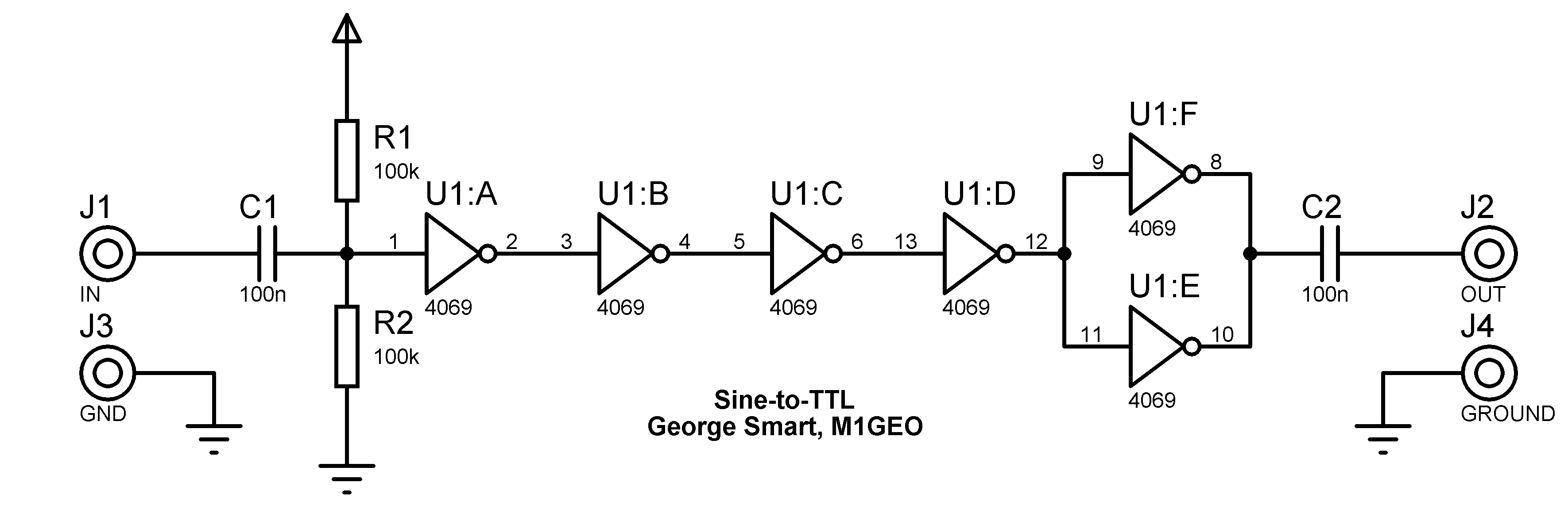
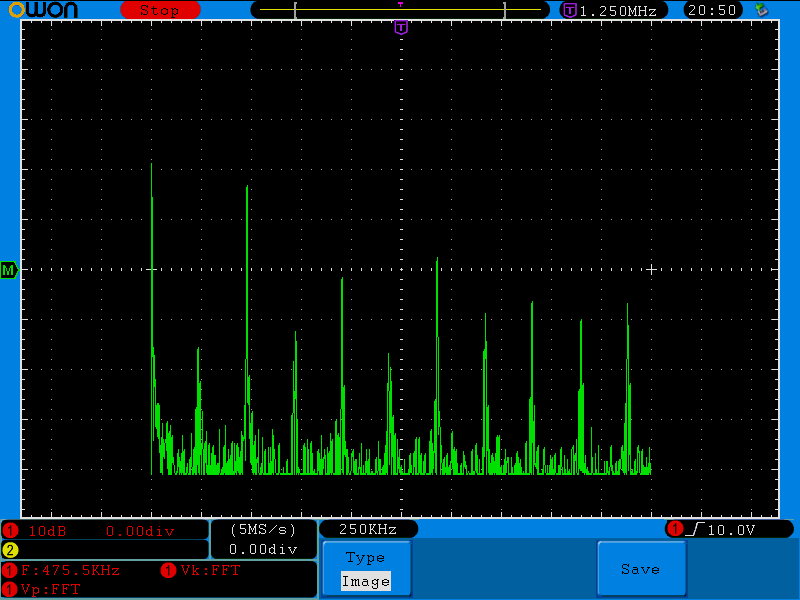
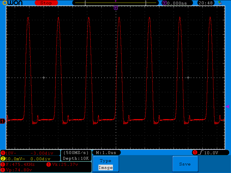
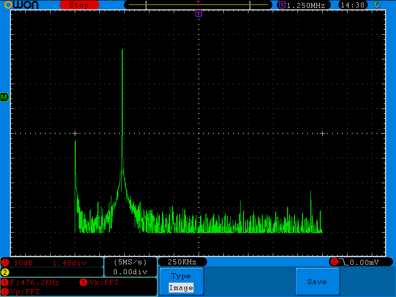
At the output of the Sine-to-TTL converter, there is a square-wave pulse train at the input frequency. This signal is fed to the FET gate, which is where this voltage train was measured. Left is the time domain, right the frequency domain via fast Fourier transform.
 |
 |
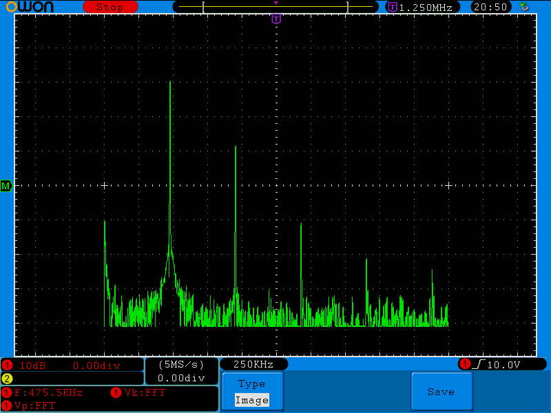
The drive on the FET’s gate is amplified. The drain of the FET has the amplified signal. The two images below show the time and frequency domain on the drain.
 |
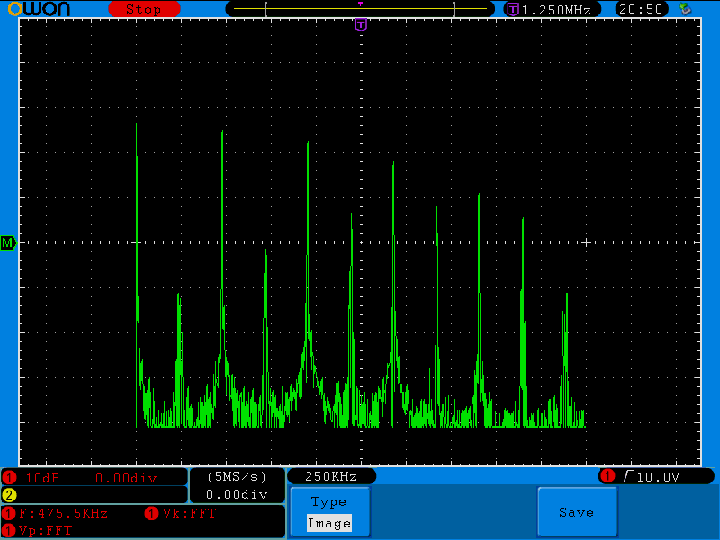 |
Finally, here we can see the filtered sine-wave output and FFT from the PA. I’m still not happy with the design, it needs a little more filtering, and a little more harmonic suppression, which is why it’s still not been on air yet.
 |
 |
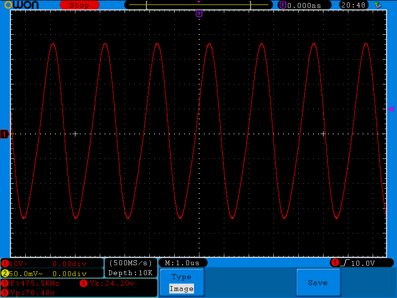
We can calculate the power into a  resistor using Ohms law. The sine wave after the filter is 70.4 Volts, peak-to-peak.


13.18 Watts dissipated into the (47 is what I had) (See my Power Calculator). GW3UEP suggests that on higher voltages, much more power is achievable. This was from a supply of 13.5 Volts with a supply current of 1.027 Amps.

This gives an overall efficiency,  , of:
, of:

Attempt 2
With increased voltage and higher current IRF640 MOSFET, I decided to remeasure the power and efficiency. I also changed the driver circuit to a transistor buffer and current amplifier from the earlier 4069 CMOS gates.
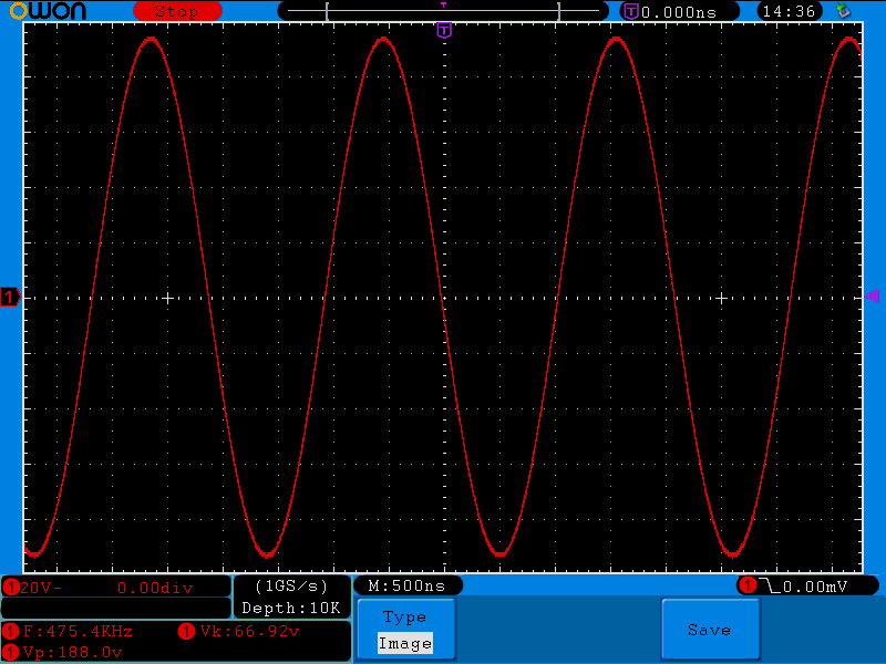
We can calculate the power into a resistor using Ohms law. The sine wave after the filter is 188 Volts, peak-to-peak.


88.4 Watts dissipated into the (See my Power Calculator). This was from a supply of 30.88 Volts with a supply current of 3.02 Amps.

This gives an overall efficiency, , of:

For a class-E amplifier, above 88% efficiency is considered to be working well. After about 5 redesigns, it finally seems like I have my high power amplifier working correctly!
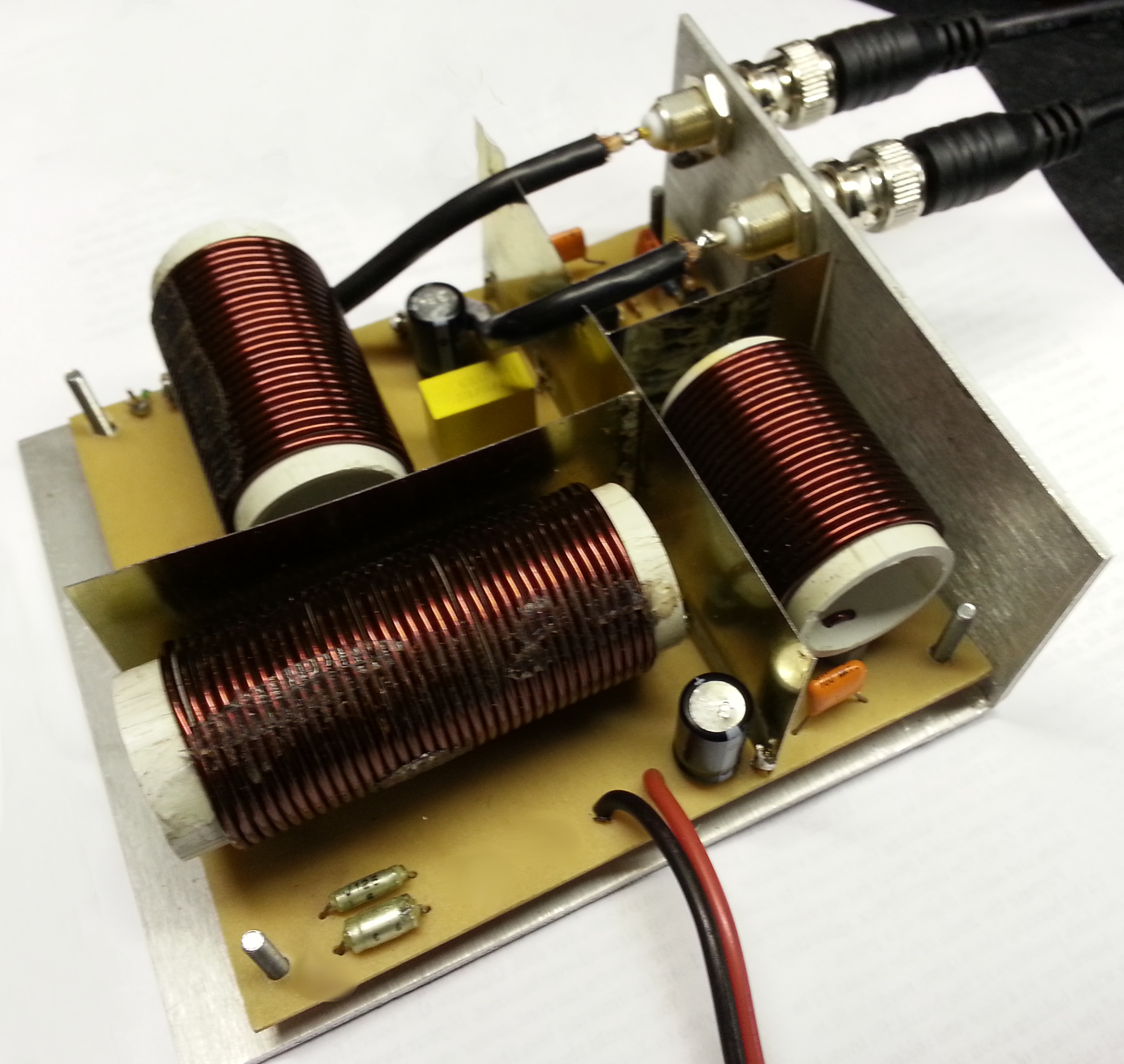
Final Amplifier
I am in the process of documenting this new amplifier! The schematic and PCB will be online shortly, but, in the mean time, here’s a sneak preview:
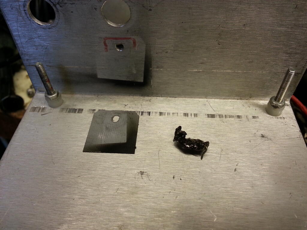
Failure
Here is probably a good place to notice that while this amplifier will do 100 Watts continuously with adequate heatsinking, if the antenna falls down, the capacitors can’t handle the voltage! This shows one that vented all over the FET and heatsink pad. You can also see the vented/melted. The FET survived okay!
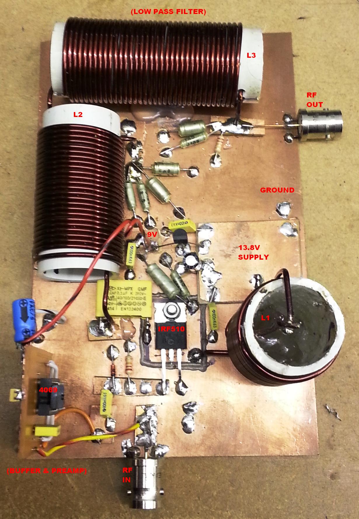
PCB Designs
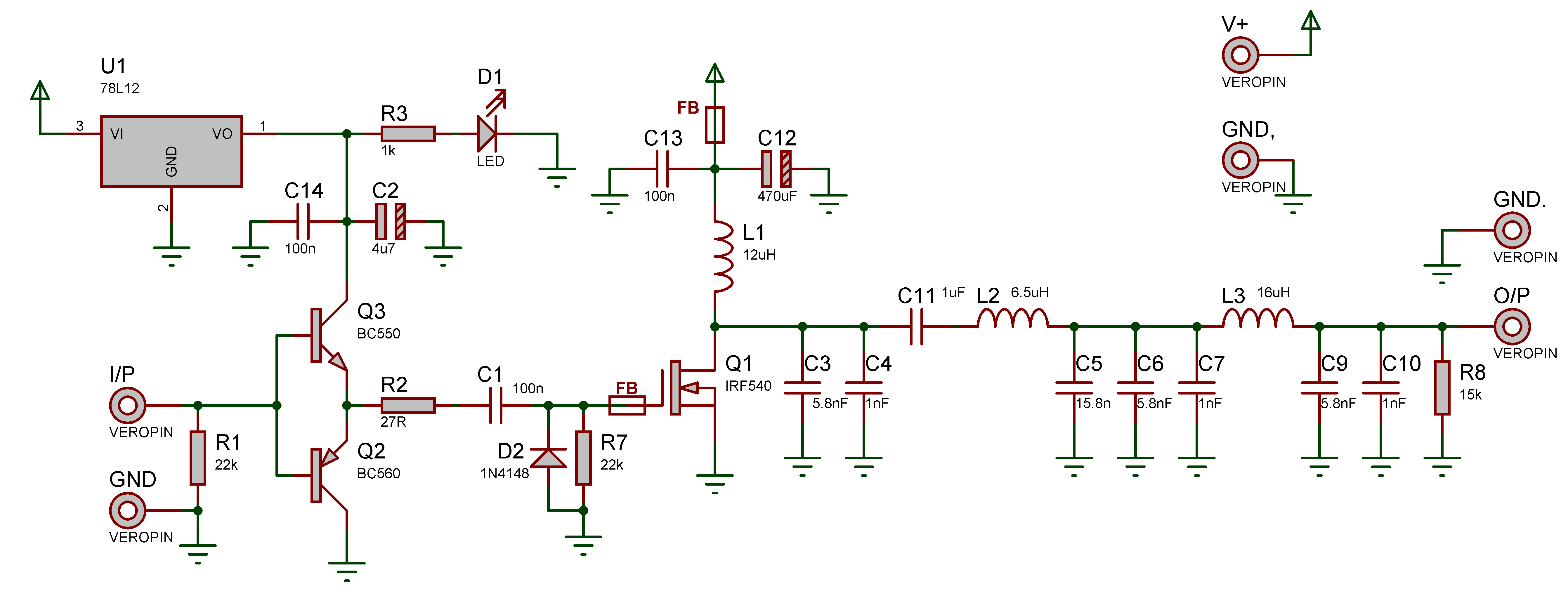
After tinkering about I decided to make a PCB. The PCB underwent a few revisions before I settled on the final version printed here. As mentioned above, the CMOS driver was replaced with two bipolar transistors to provide sharp square pulses to the FET. This improves the efficiency of the amplifier. The current working schematic (as of 20/10/2013) is as follows:
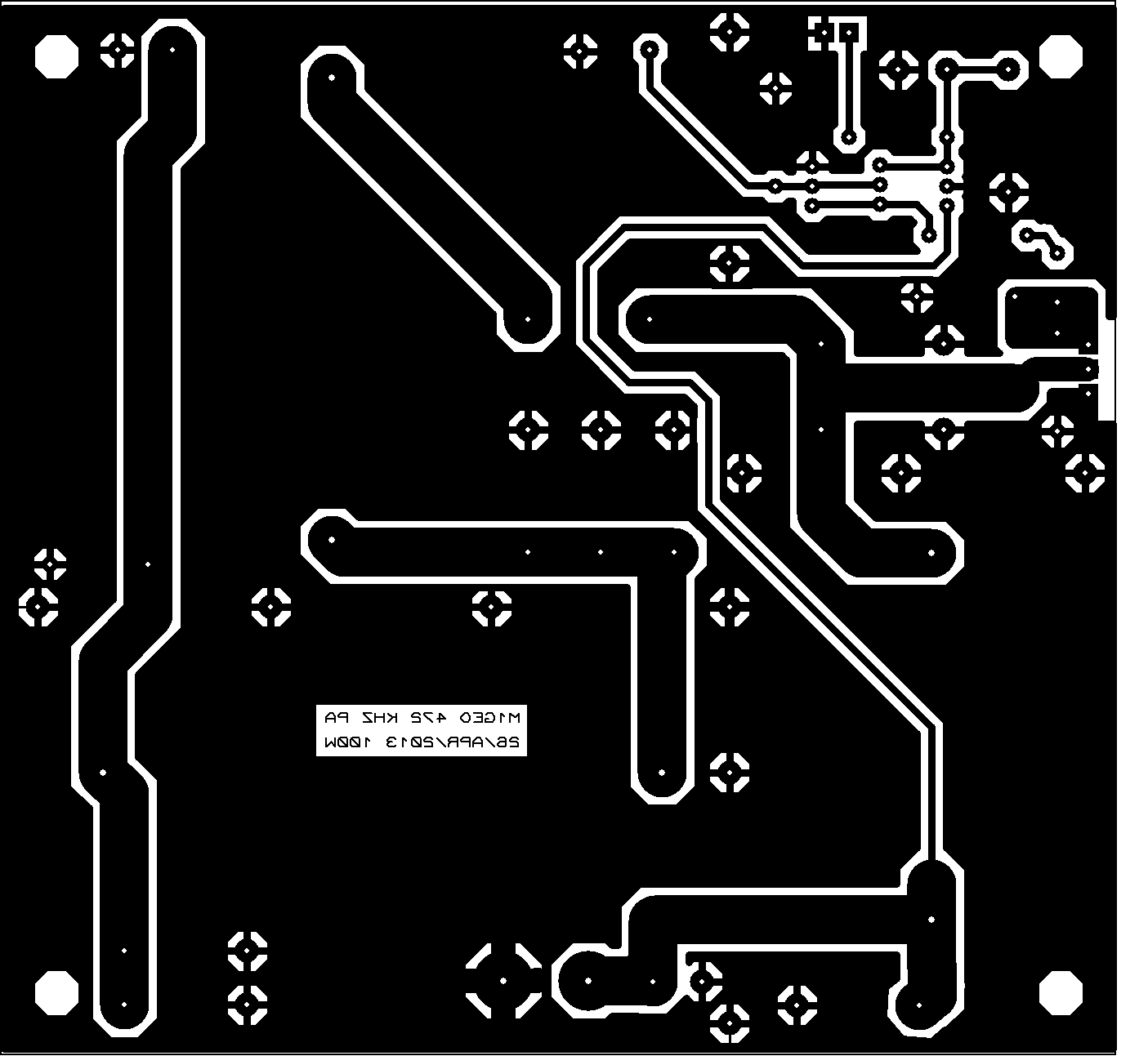
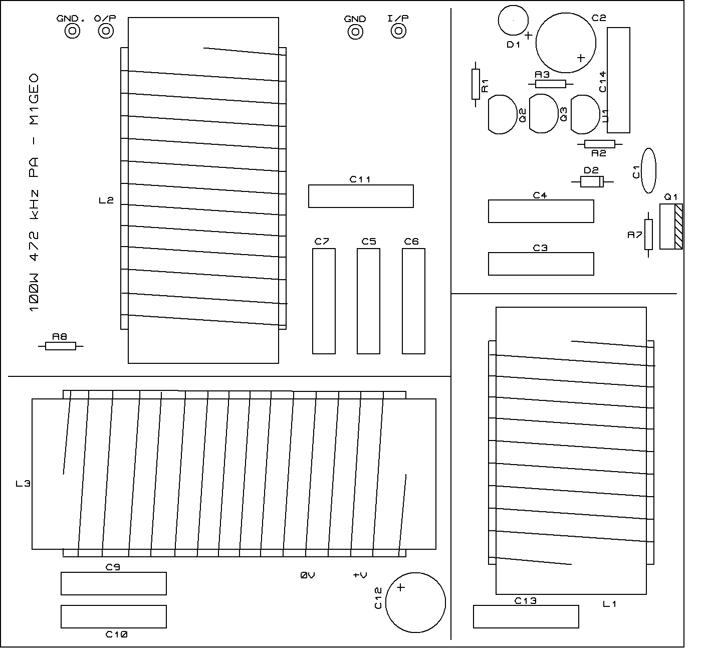
And the complimentary PCB copper and silks at 300 DPI:
Low Pass Filter
After having about 10 attempts at building a low pass filter, I found out that the Micrometals ferrites that I was trying to use (T130-52) were in fact Chinese copies of the Micrometals which appeared the same visually, but did not perform at all well. Micrometals have issued a warning message about ferrite ring copies. I have since done some measurements of the toroid cores.
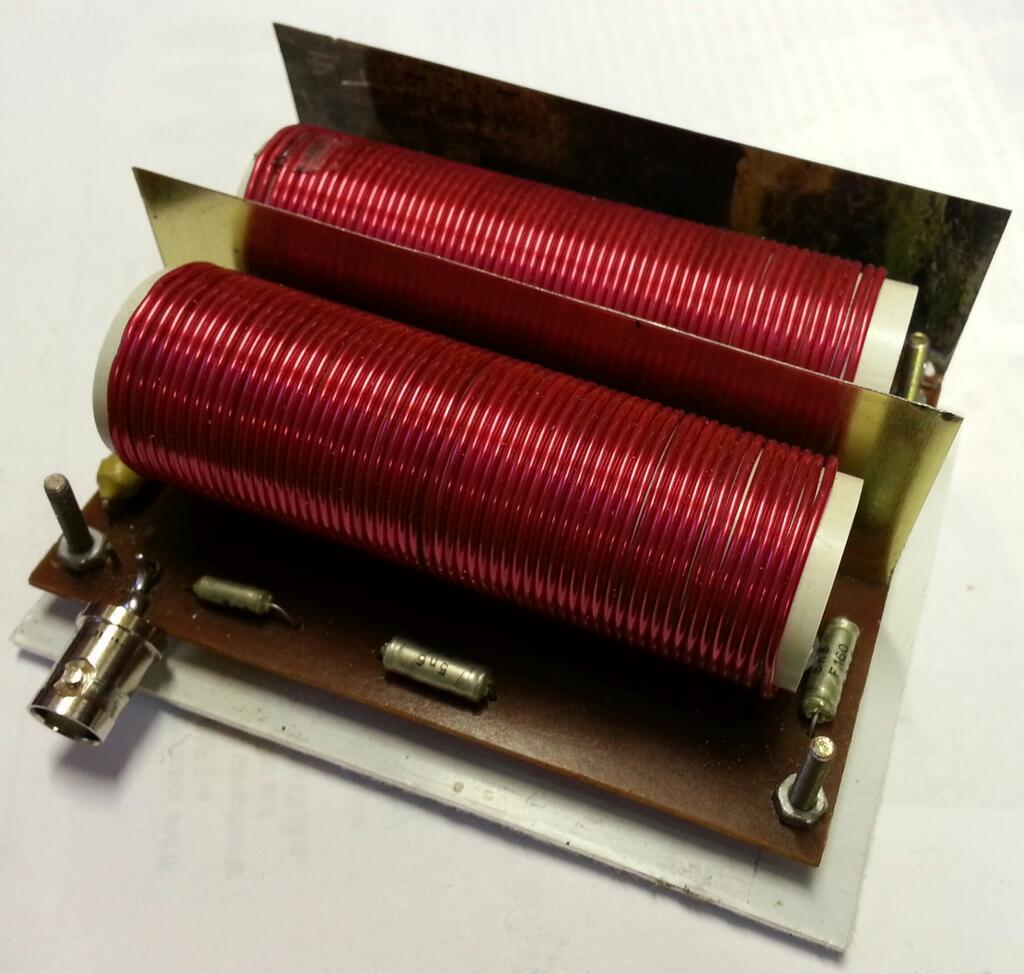
The image below was taken with the only camera available at the time and is accordingly awful. I will try and get a better picture soon!
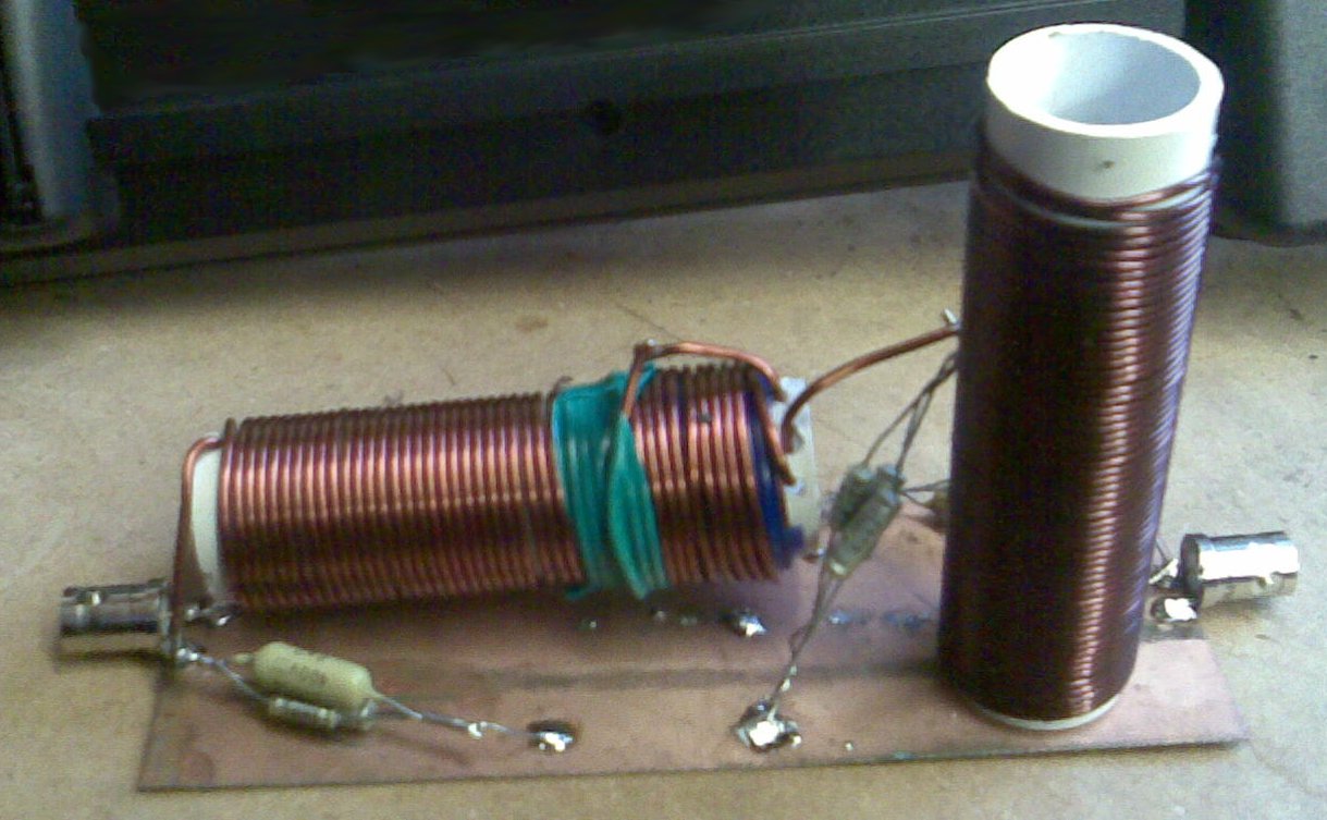
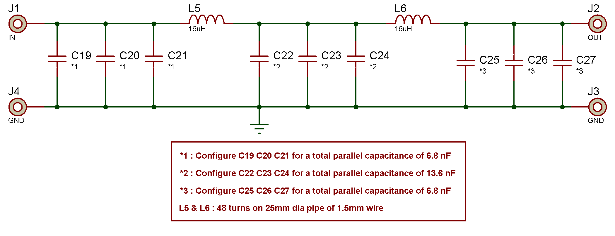
The LPF we settled on is an 5th order Chebyshev filter, designed with the AADE Filter Design Software. it is implemented using two air-core inductors wound in the same construction style as the PA and 3 capacitor poles made from high quality capacitors capable of handling the power.
The filter’s frequency response is shown below:
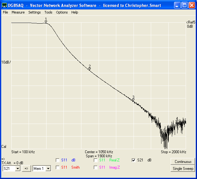
The markers on the graph are at the harmonics of the band centre, and where I do 472 kHz WSPR.
# 475 kHz : -0.66 dB
# 950 kHz : -37.91 dB
# 1425 kHz : -62.38 dB
# 1900 kHz : -79.26 dB
These values are just the filter. The PA already has a 5th order Chebyshev filter and matching network of it’s own. The final two scope prints show the output of the LPF with the PA driving into a load.
 |
 |
Last of all, I decided to make a proper PCB up and screen the coils from each other. The final picture shows the “finished” low pass filter.
Stand alone filter design files:
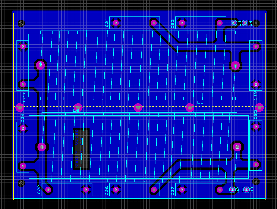
Finally, two PDFs for the board layout. These are correctly scaled, so turn off any scaling inside your PDF viewer, i.e., print at 100% with an A4 paper selected (as this is the correct aspect ratio).