
I have had my Yaesu FT-2800M for about 3 years. I bought it second hand at a radio rally and it has, until now, given me years of faithful service. While in a recent QSO I noticed that the power output had dropped to nothing. Googling around revealed that this is a common fault with the FT-2800. As you may have gathered from other pages on this site, that I am reasonably technical, and so I decided to do the repair myself. This page is offered to show you how I did it; more what’s involved in doing this yourself. I only needed to replace the final transistor, but the driver is replaced in exactly the same way.
The job is fairly simple if you’ve used a soldering iron before. You’re dealing with power electronics, and so the soldering is big stuff. Nothing too fiddly. The service manual for the FT2800 is here.
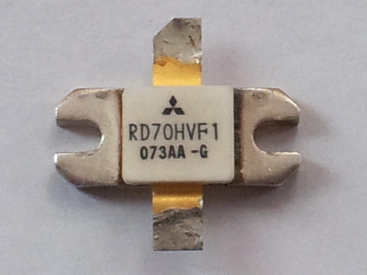
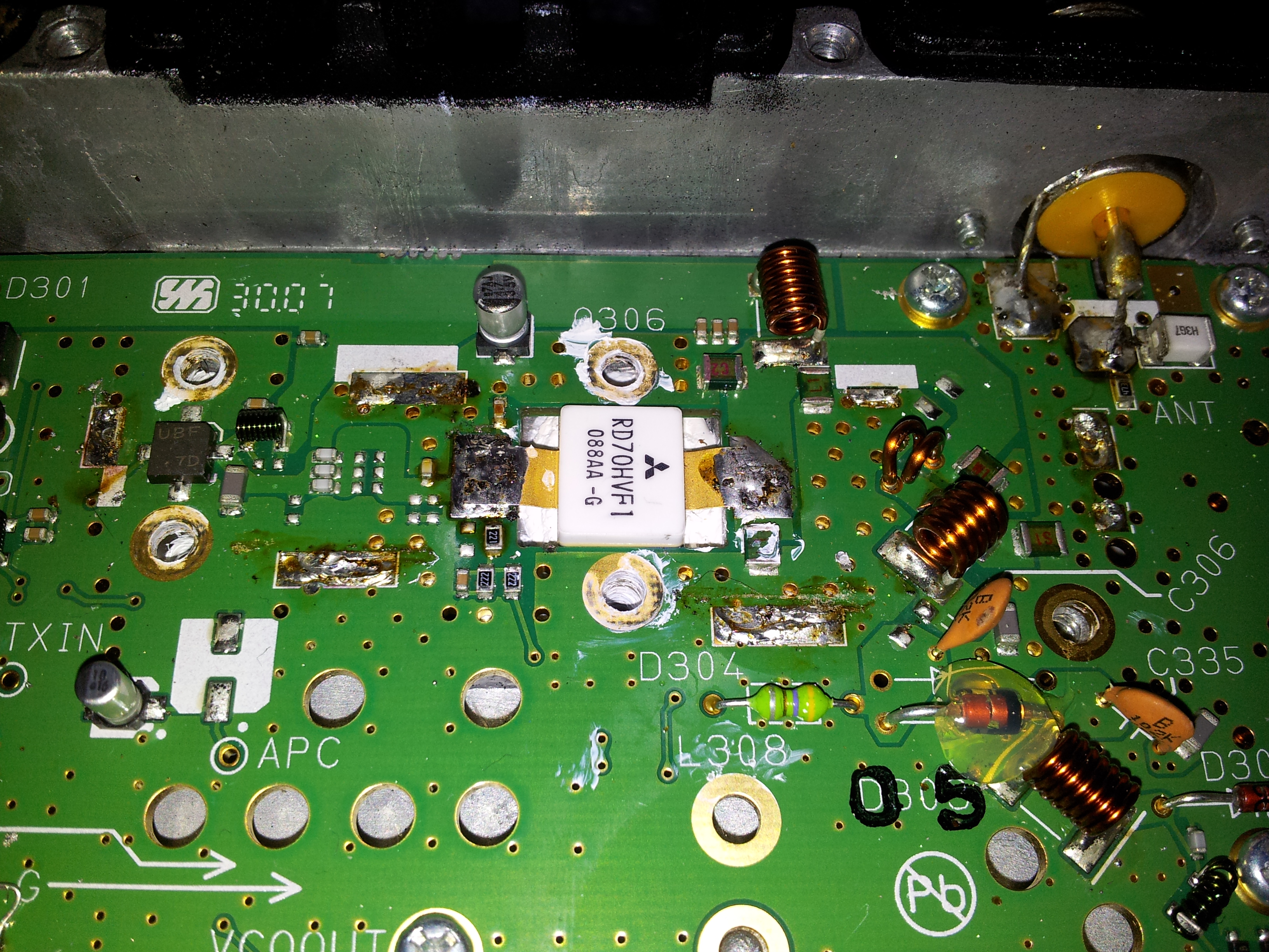
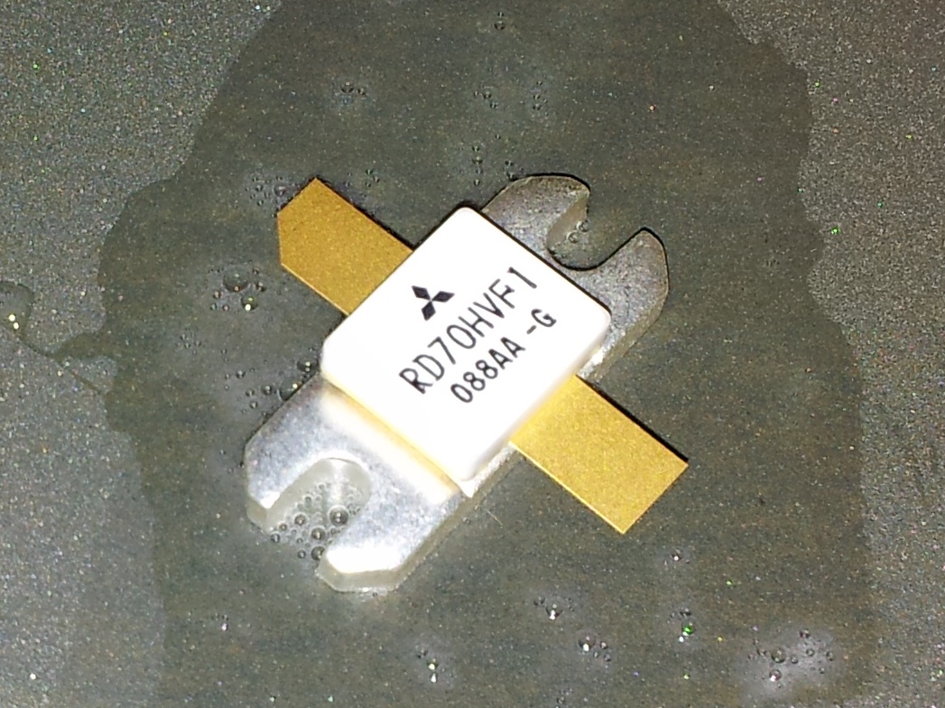
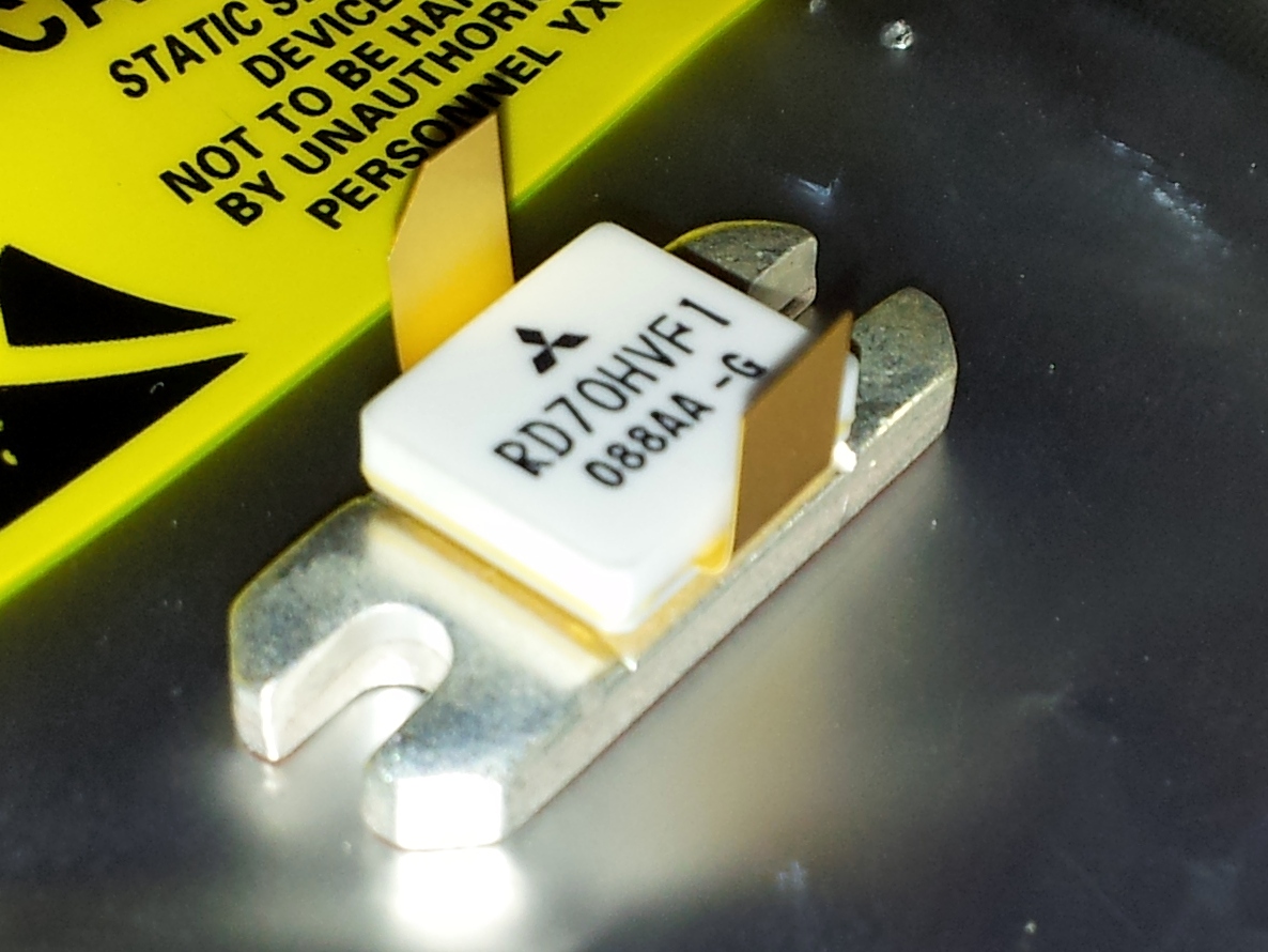
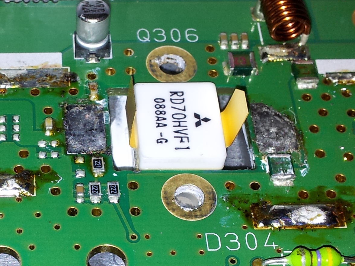
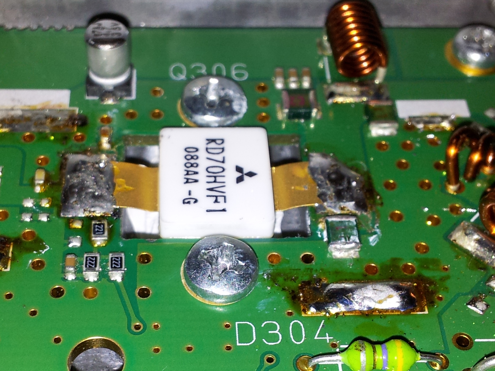
The transistor you are looking to replace. It’s a Mitsubishi RF power MOSFET RD70HVF1 (datasheet for part here). In the FT-2800, it’s transistor Q306 on the PCB and Yaesu’s part number for it is G3090140. Check these numbers though, I may be wrong! It is electrostatic sensitive, so don’t go touching the pins of the FET if you can help it. You don’t want to kill it!
 |
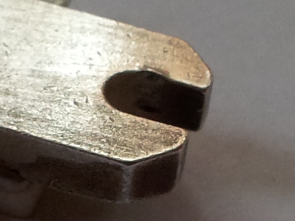 |
From looking at the removed part (above left) you can see, and easily feel, a burr around the outside of the mounting holes (above right). This is where the device meets the heatsink. Very good contact between the FET and heatsink is required to transfer heat away from the FET. This burr lifts the FET from the surface of the heatsink very slightly but greatly reduces heat transfer. The device would have cooked itself – there is evidence of this in the black charring on the metal surface around the ceramic (white) top of the FET in the above left image.
I ordered my replacement part from eBay. Double check that it is (a) a genuine Mitsubishi part, and; (b) that it is the correct part (Mitsubishi RD70HVF1 for the Yaesu FT-2800M – check your rig uses the same part). I paid around £20 delivered from Hong Kong.
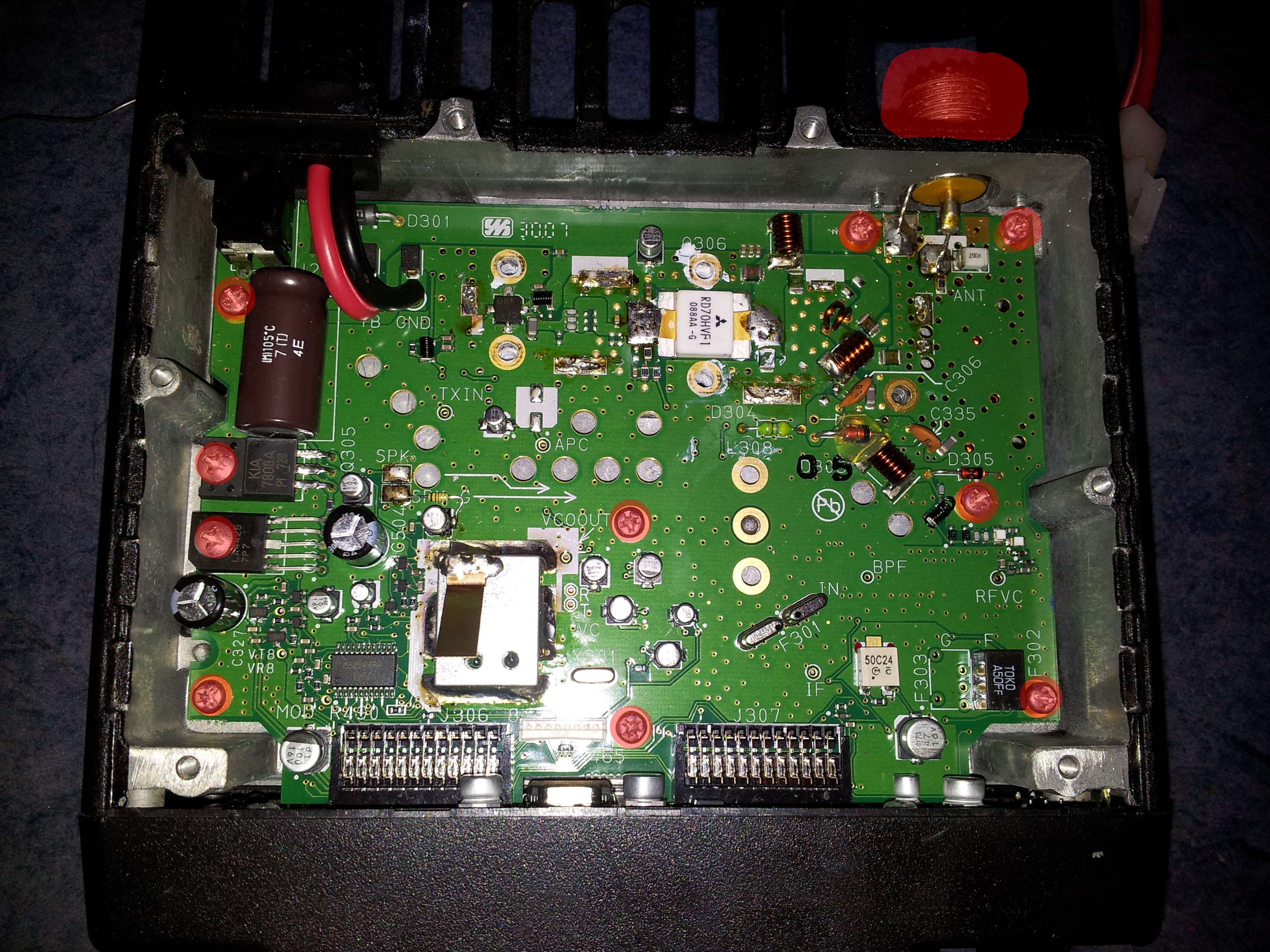
Remove the 6 screws holding the bottom plate on. There are 4 screws and two feet also screwed on. The bottom plate will lift off. Set the backplate aside.
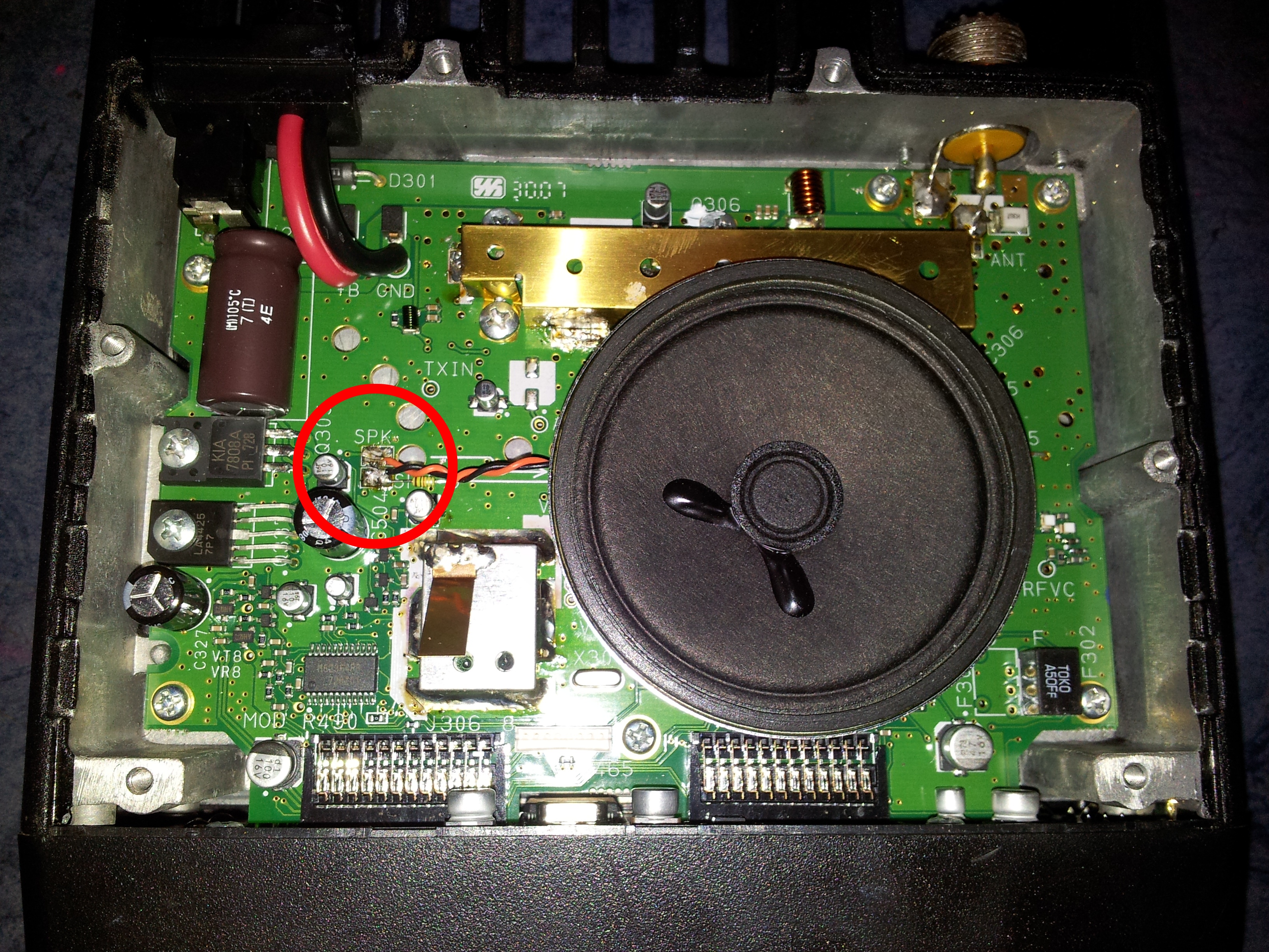
I removed my speaker. It’s soldered on with 2 wires, clearly labelled SPK on the PCB. Usually this would be a case of removing a connector, but these are cheap radios and so there’s not that luxury. Set the speaker aside. You don’t have to remove it, but it will get in the way and probably break the wires anyway, later.
 |
 |
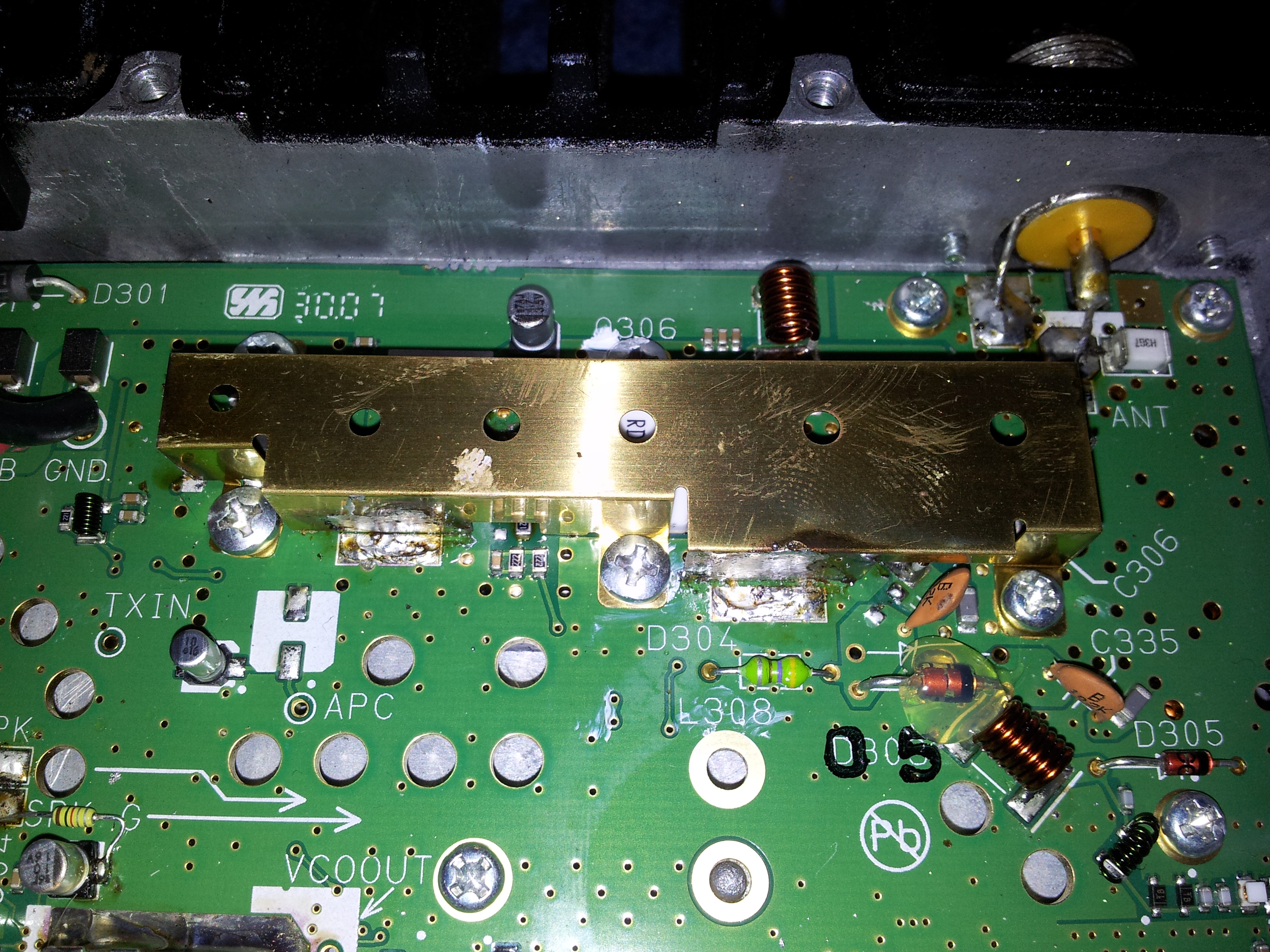
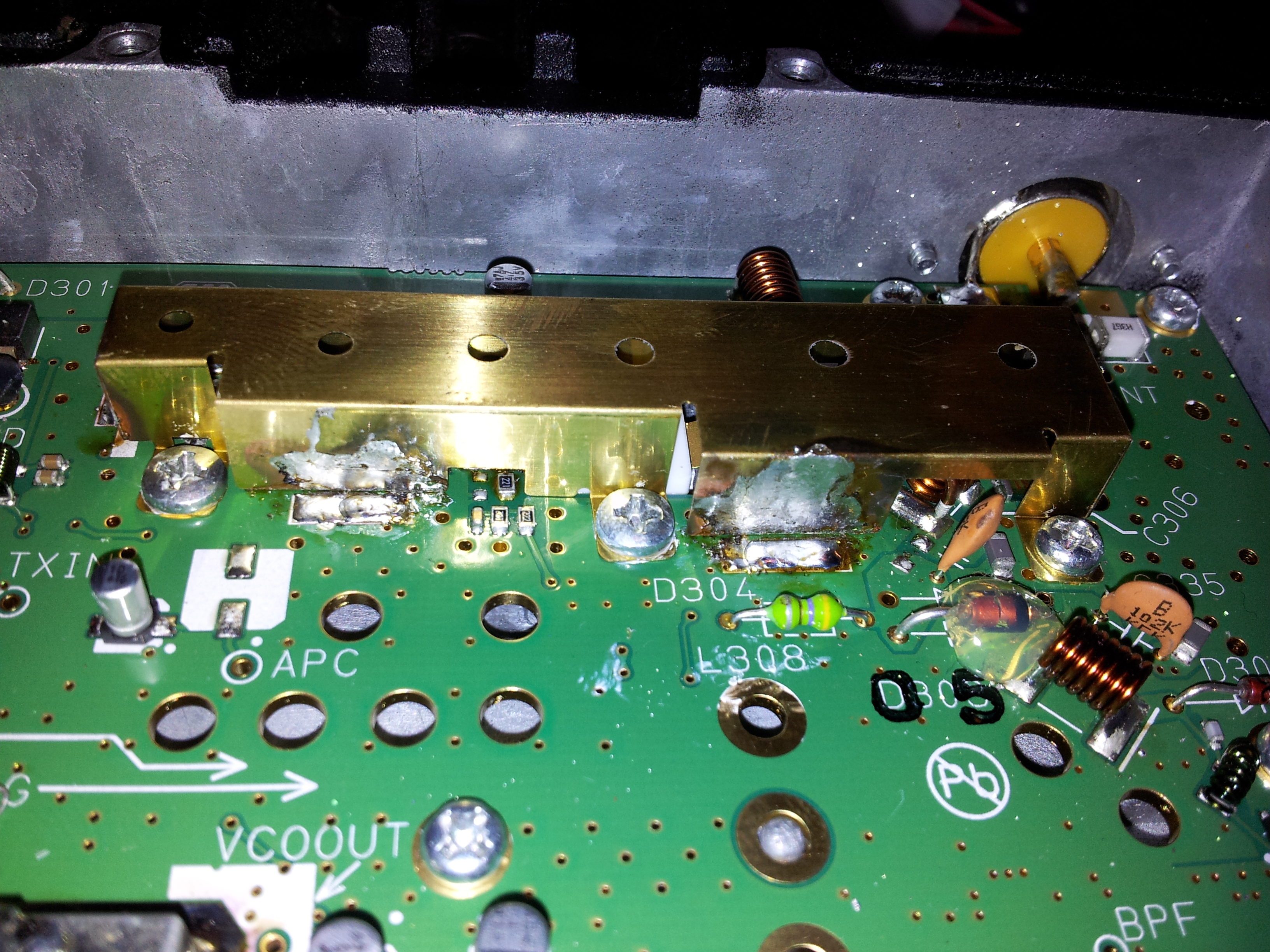
The final hurdle to remove the PA transistor is to take the mainboard out of the radio. The PA transistors are sandwiched between the PCB and the heatsink. You need to lift the PCB. Remove all the screws holding the board down. This includes the two holding the voltage regulator and audio amplifier, next to the large capacitor on the bottom left (front panel toward you) – these are slightly larger screws than the others holding down the PCB. I also removed the coax connector on the back. The pin that sticks out on the inside makes it hard to lift the board. The SO239 is held on using two screws, the same as held down the voltage reg and the audio amp.
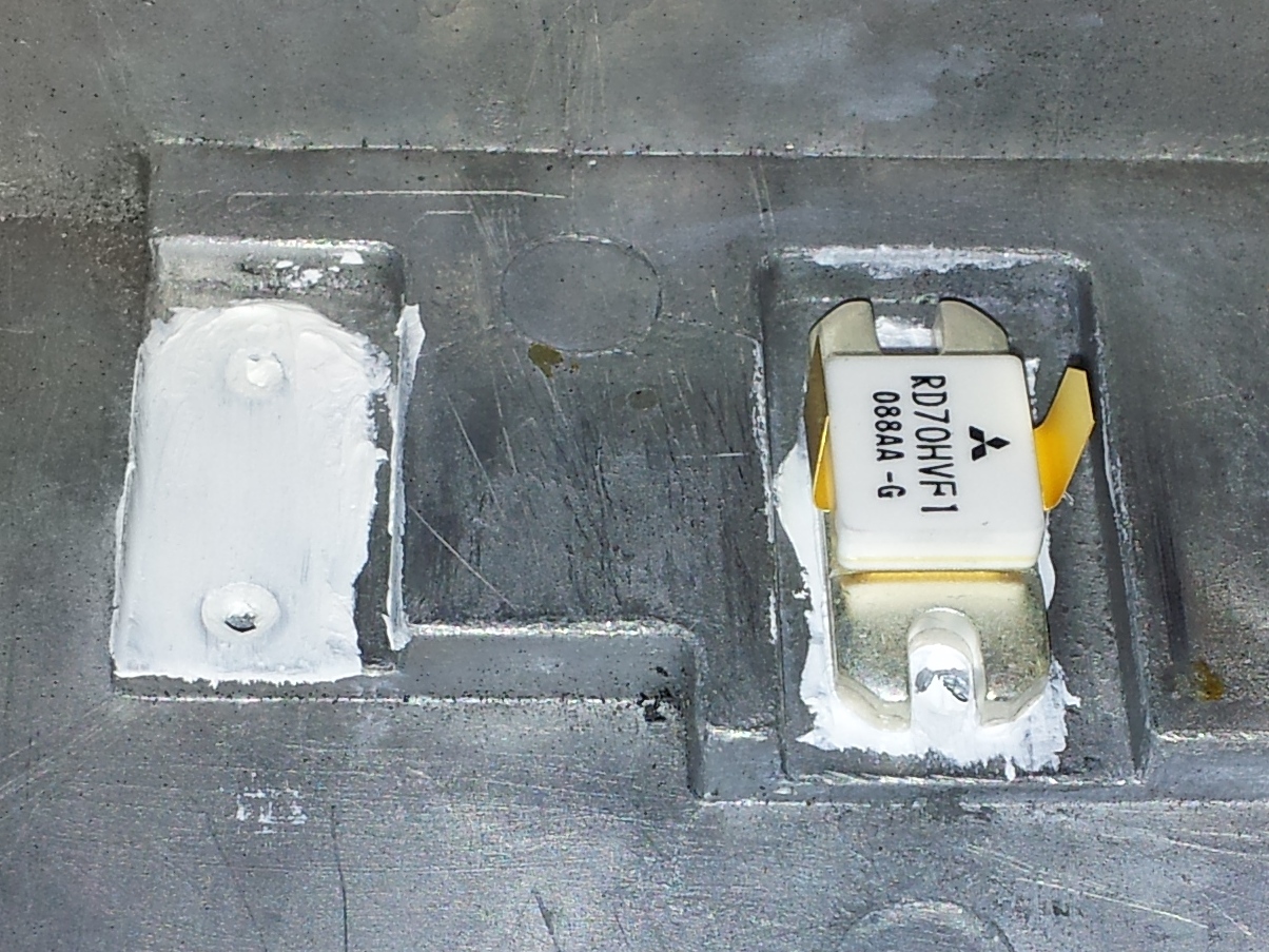
Clean the heatsink compound from the heatsink and check the metal has a very smooth finish. DO NOT scratch the area of the heatsink under the transistors
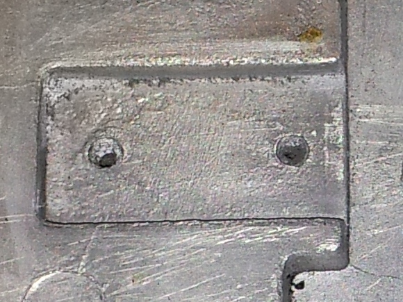
! My chassis & heatsink had massive burrs around the screw holes, that had pushed up the transistors, compounding the overheating problem further. I used a very lightly abrasive sand block, and rubbed the burrs away. I was appalled at this. No wonder the PAs burn out on these! Here’s what the cutout for the final FET looked like on my FT-2800M.
You want these cut outs to be a mirror surface. That comes with a good deal of sanding! This is what makes the difference. You need a nice smooth surface on the FET and a nice smooth surface on the heatsink. This allows for maximum contact area, therefore lowest thermal resistance, and therefore no more blown PAs! Spend the time to do this right – otherwise you’ll add this page to your bookmarks! 🙂
Once you’ve got the chassis smooth, set it aside, and turn to the PCB. We need to remove the old final FET. This is a fairly easy thing to do. Heat one of the two solder pads until the solder melts. Then, either twist the FET slightly so the melted side separates from the board, and slide the soldering iron bit into the gap to separate the lead from the pad. Repeat this for the other pad, and remove the FET. I suggest marking it that it’s dead in some way. A felt tip penned ‘X’ on the back does for me. You’d hate to install the wrong one back! Clean the pads up so there is no solder on the pads. I only had trouble with the final stage, so I left the drive alone. If you are replacing the driver (the smaller transistor) then repeat the process for that FET too.
Next, you need to prepare the final FET. For this, I used some emery paper on a hard surface (ideally glass). Wet the emery paper, lay it on a hard flat surface, and carefully polish the back of the final FET (below, left). Once finished, it should feel smooth to the touch, just like the chassis you cleaned up previously. Note here, that you need to be careful of the other leads on the FET. It is static sensitive. After sanding the back smooth, bend the other leads to they’re loosely right-angled (pointing upwards, below right) – this is so the leads will fit through the hole in the PCB.
 |
 |
At this stage, you need to apply the heat-sink compound. You need this, it isn’t optional. It improves the thermal conduction between the PA FET and the chassis of the radio. Apply a thin layer to the back of the FET and a thin layer to the area of the chassis. If the device is fitted already, such as my driver, apply to both sides. For the final FET, which is loose, place it such that the mounting holes on the FET align with the holes in the chassis. Note the correct orientation. The RD70HVF1 has a corner cut from one of the leads. This matches the corresponding pad on the PCB. GET THIS RIGHT! If you’re fitting the driver, then do the same, aligning the mounting holes while noting the orientation.
Now fit the main PCB again. Make sure to fit the pins from the front panel into the mainboard. Drop the board home, and wobble it to seat it fully. If one of the transistors in the PA is already soldered, then use two screws to bolt it down. It is important that the board isn’t twisting the FETs, so by fitting presoldered FETs first, it ensures that it will be seated correctly later. I screwed the driver down. Then fitted the board’s standard holding screws, refitted the SO239, audio amplifier IC and voltage regulator.
Finally screw down the new FET. It should all align with the pads. Tighten the screws at each end in a balanced way. 1/4 of a turn on each screw, repeating until tight. This gives the heatsink compound a way to escape and ensures an even layer. Finally, solder down the final FET. My method is to tin the tips of the FET legs. Then pool a little solder on the pad, and using a fine screwdriver, push the pad down into the pool, holding until set.
 |
 |
Once it’s soldered in, refit the cover. Be sure to solder the metal can down once you’re sure that everything is correct. Then perform the alignment procedure for the transmitter as outlined in the service manual (above).
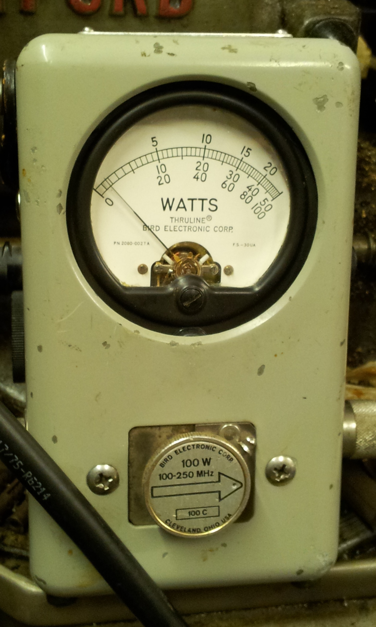
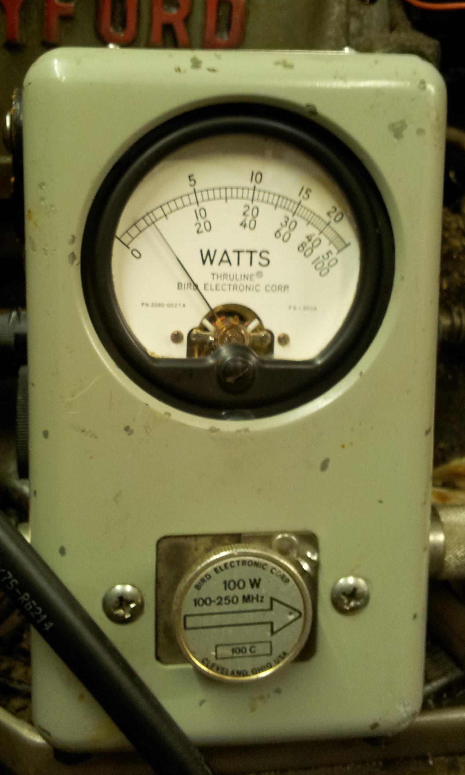
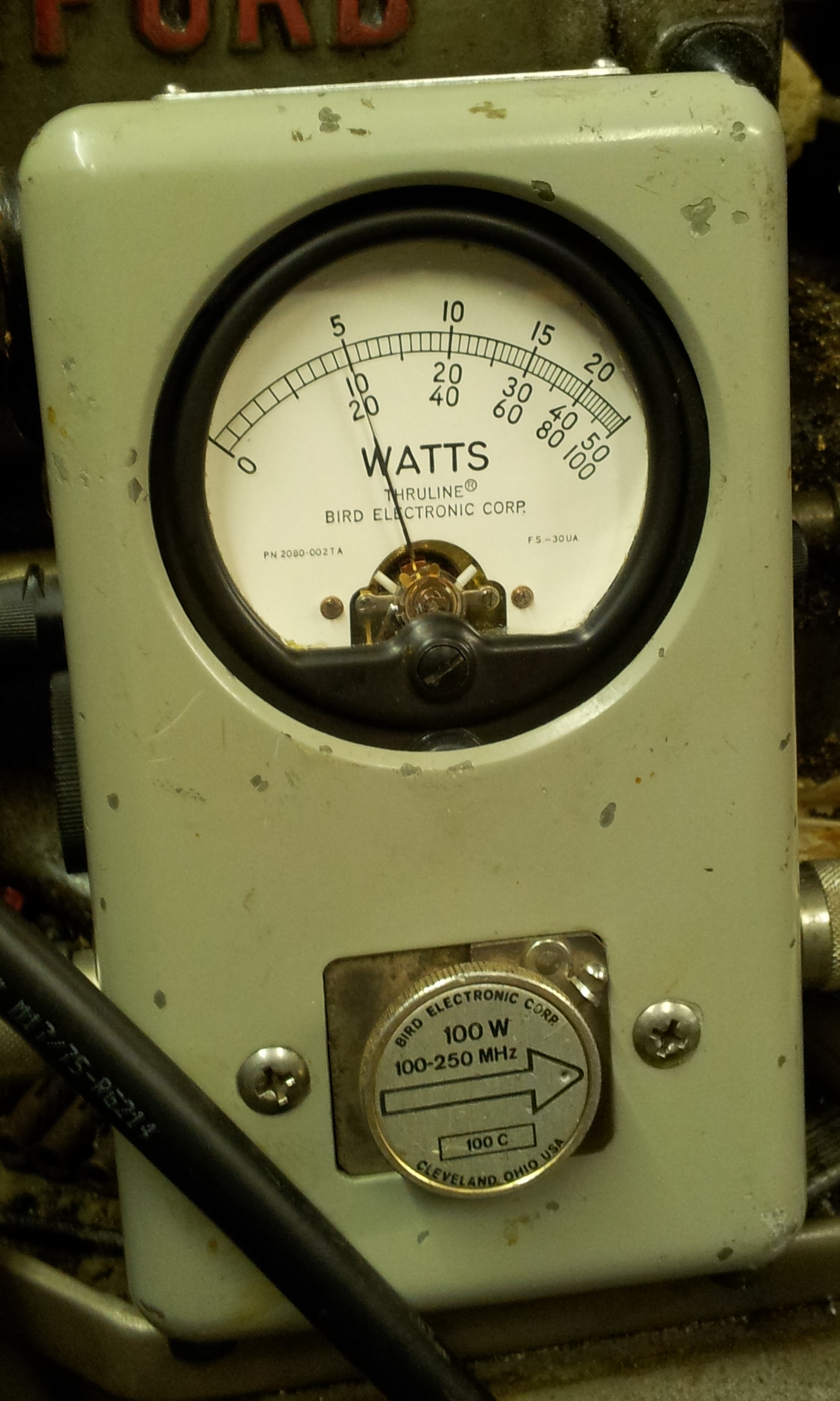
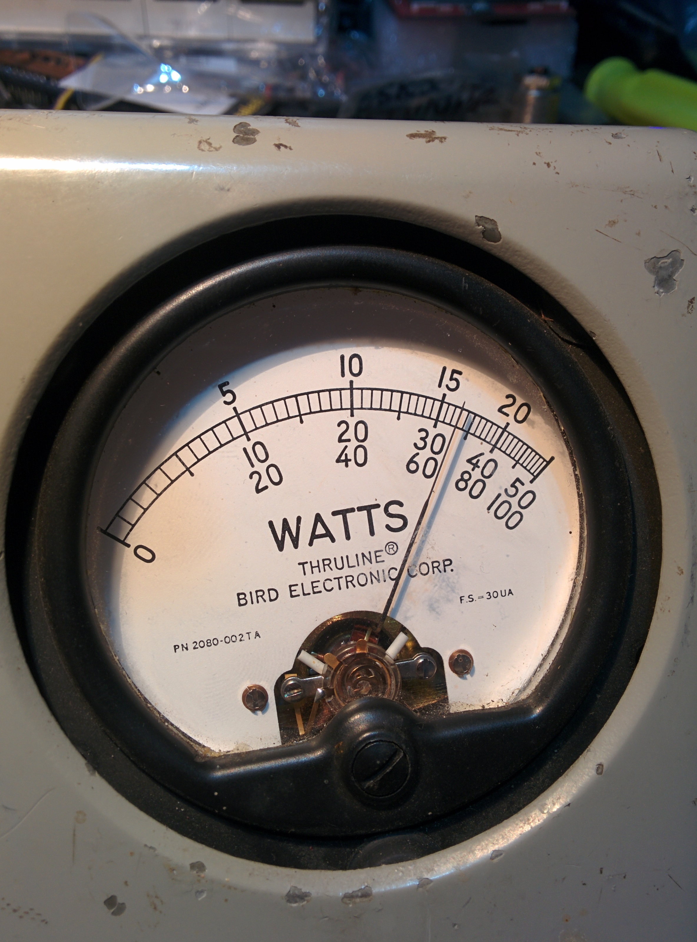
All that remained was to give the rig a quick test. Connected to a dummy load, the power output was measured using a Bird ThruLine.
 |
 |
 |
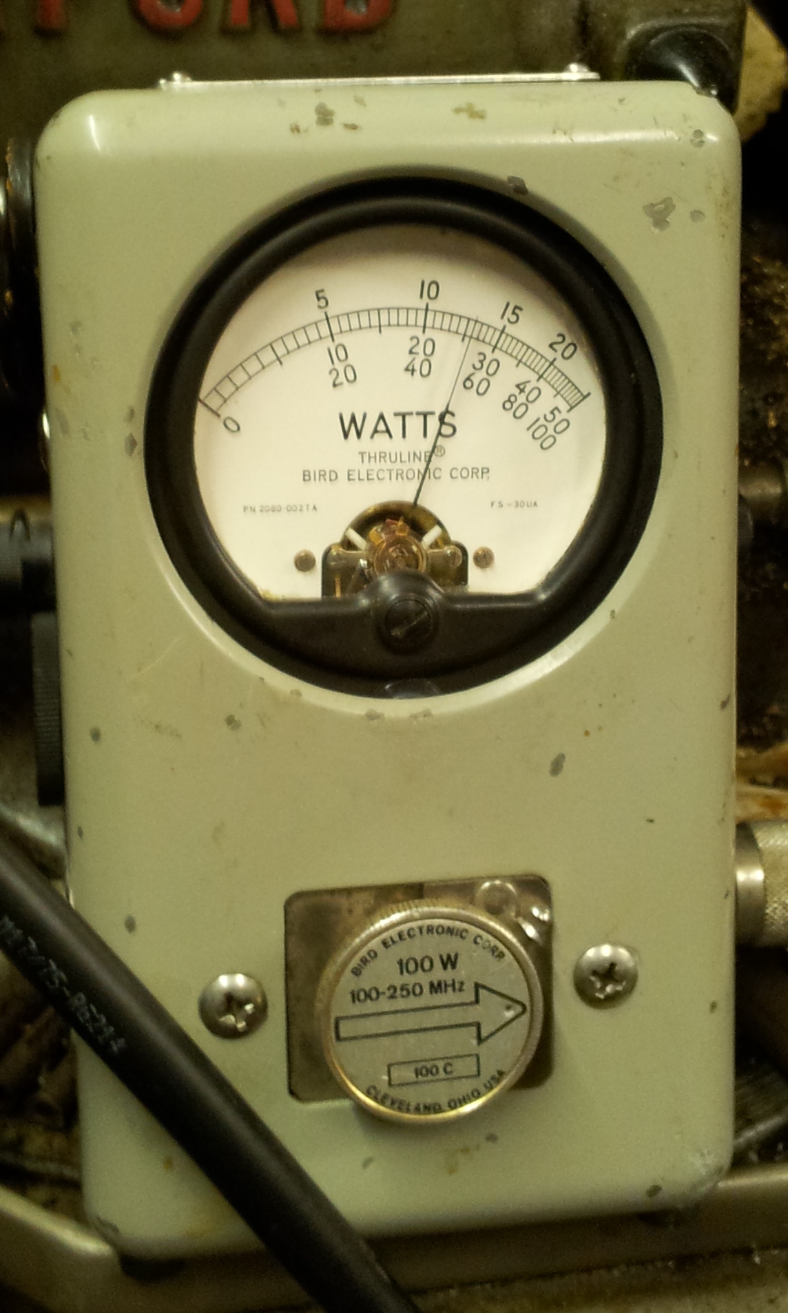 |
| 5 Watts setting | 10 Watts setting | 25 Watts setting | 65 Watts setting |
You may notice the radio is producing slightly less power; this is because of a low supply voltage. I later checked on a better regulated 13.8 volt supply and received the full 65 watts Yaesu state.
Driver Replacement
Some time after the replacement of the PA transistor, the driver went – the radio spent about 4 years in its box because I had no interest in working on it – it frustrated me! Anyway, in the process of clearing out the shack I came across the radio again, and figured now it had no real value to me, it’d be worth a shot. I wasn’t too worried if I killed the rig, since it was no use as a TX and I didn’t trust it anyway.
I did a few tests: with a scope I could see there was signal going into the driver, and not coming out of it – i.e., the driver was attenuating. As a crude tell-tale test, I bypassed the driver stage with a 100pF capacitor, and transmitted, and I got about 6W out on maximum power. This was what I was expecting. The radio is 65W, and the driver is around 10dB. In bypassing the faulty driver, the PA strip looses 10dB of gain, so it’s 65W becomes 6.5W. This implies the final stage is working, but the driver is dead. I decided to gamble I could fix it, and ordered the part…
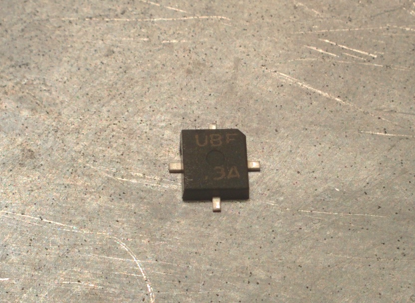
The driver is Q313, a Toshiba 2SK3075 RF Power MOSFET (datasheet for part here) for VHF/UHF, Pout>=7.5W, G>=11dB. This is surface-mount device which is soldered to the copper heat-spreader – be careful with a very hot iron! I picked up 2 driver parts online for around £5 each from a reputable supplier. Beware of Chinese fake PA transistors, which (to my experience) are re-badged 2N2222’s 🙂
 |
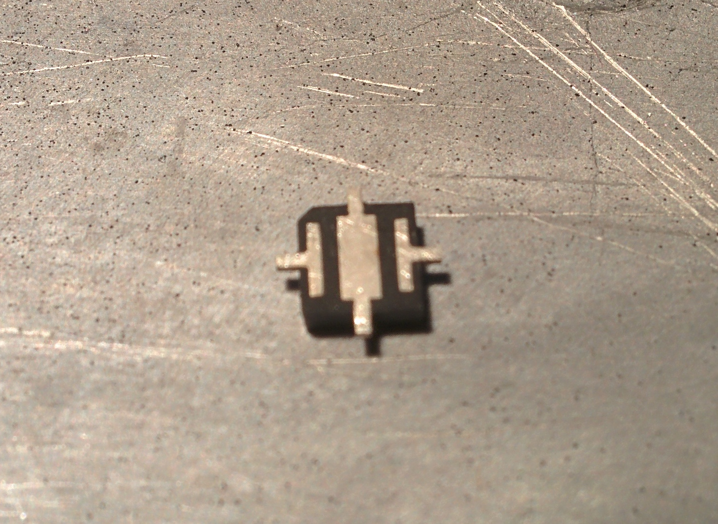 |
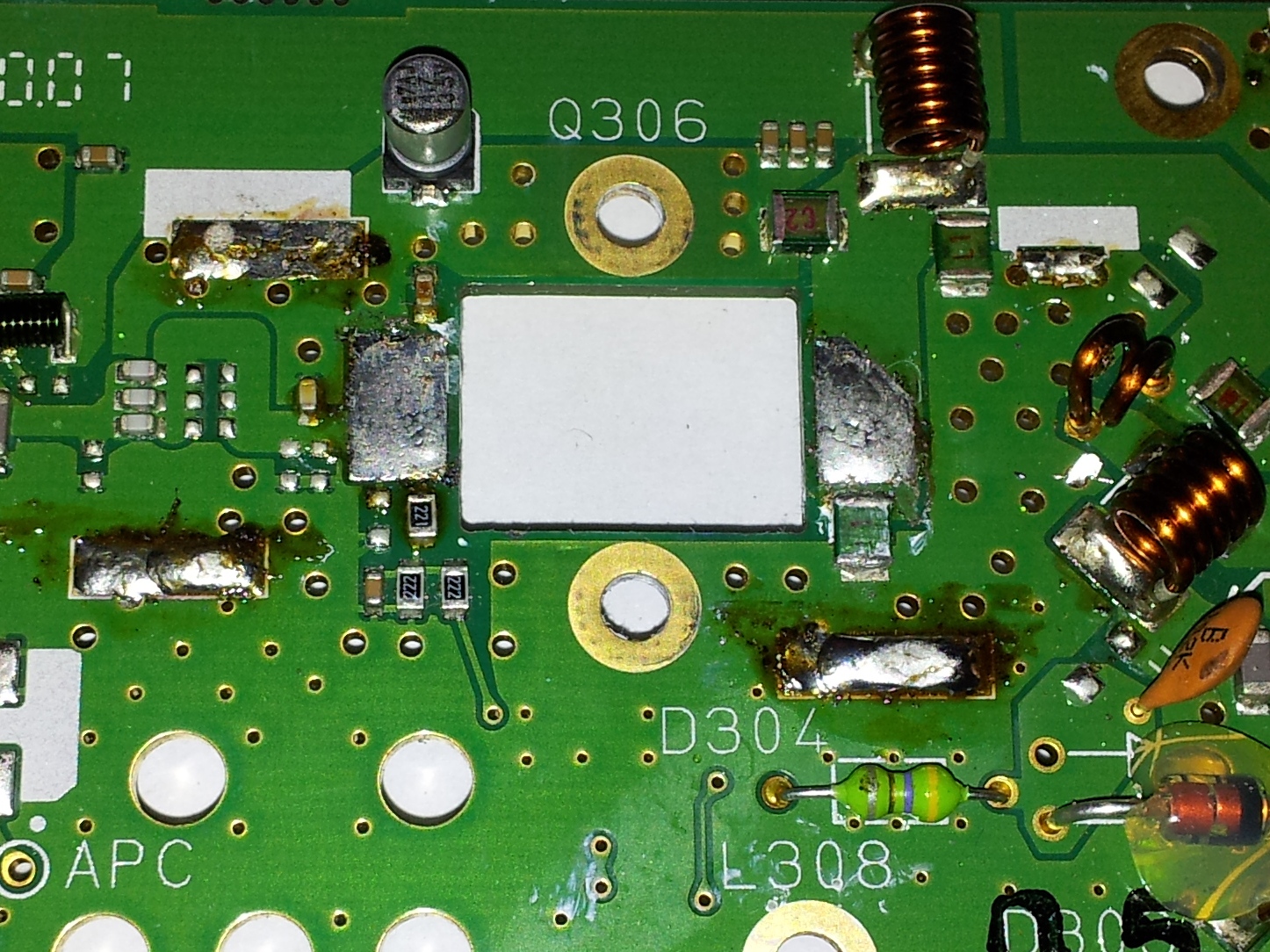
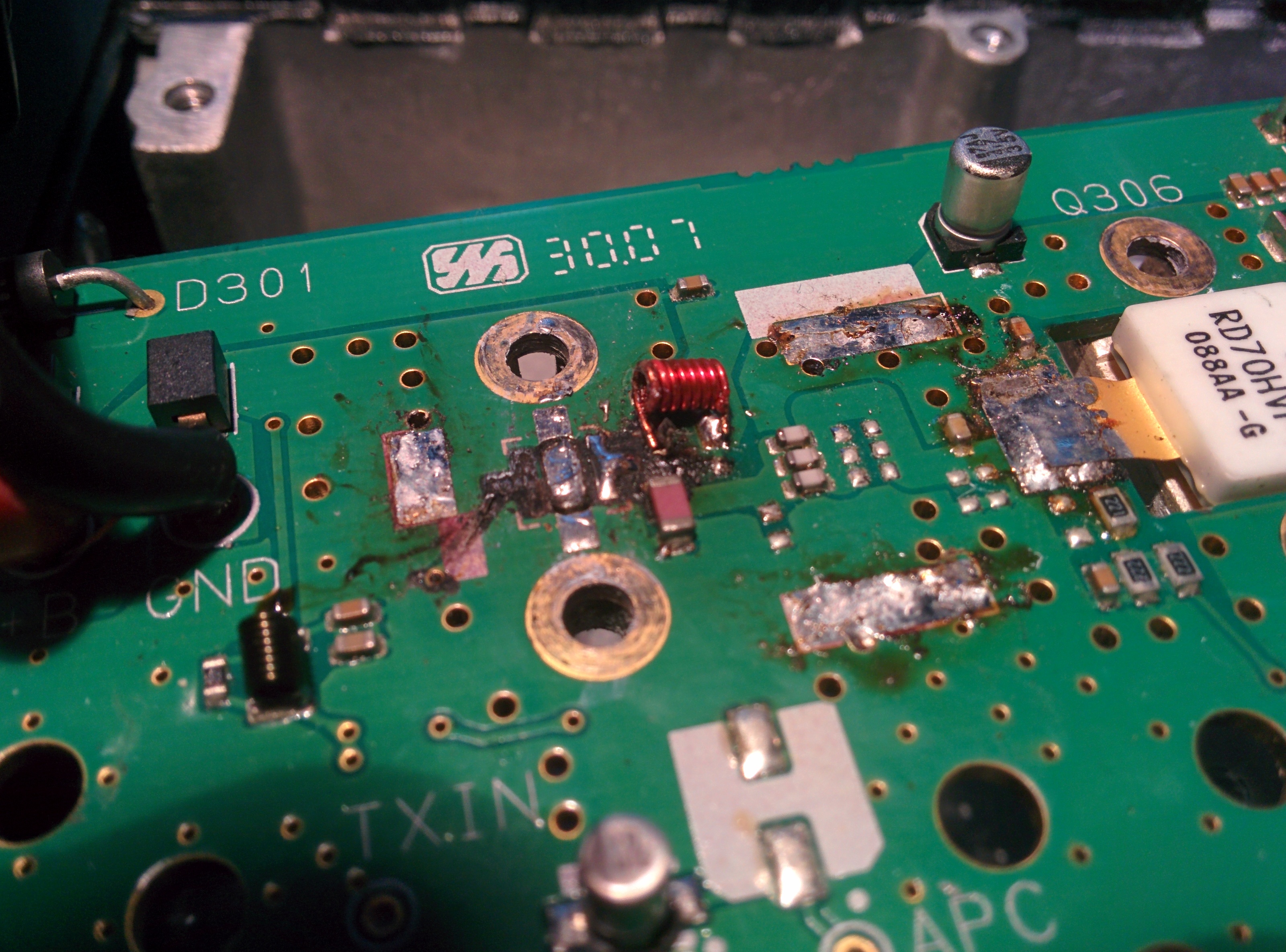
The existing part is very hard to remove because it is soldered to the copper heat-spreader, as mentioned. I had to destroy the old part to remove it. I used a very hot iron to then clean the central (heatsink) pad up. The image below shows the mess I made of it – extra care should be taken not to lift the gate and drain track pads (as I did on the gate!).
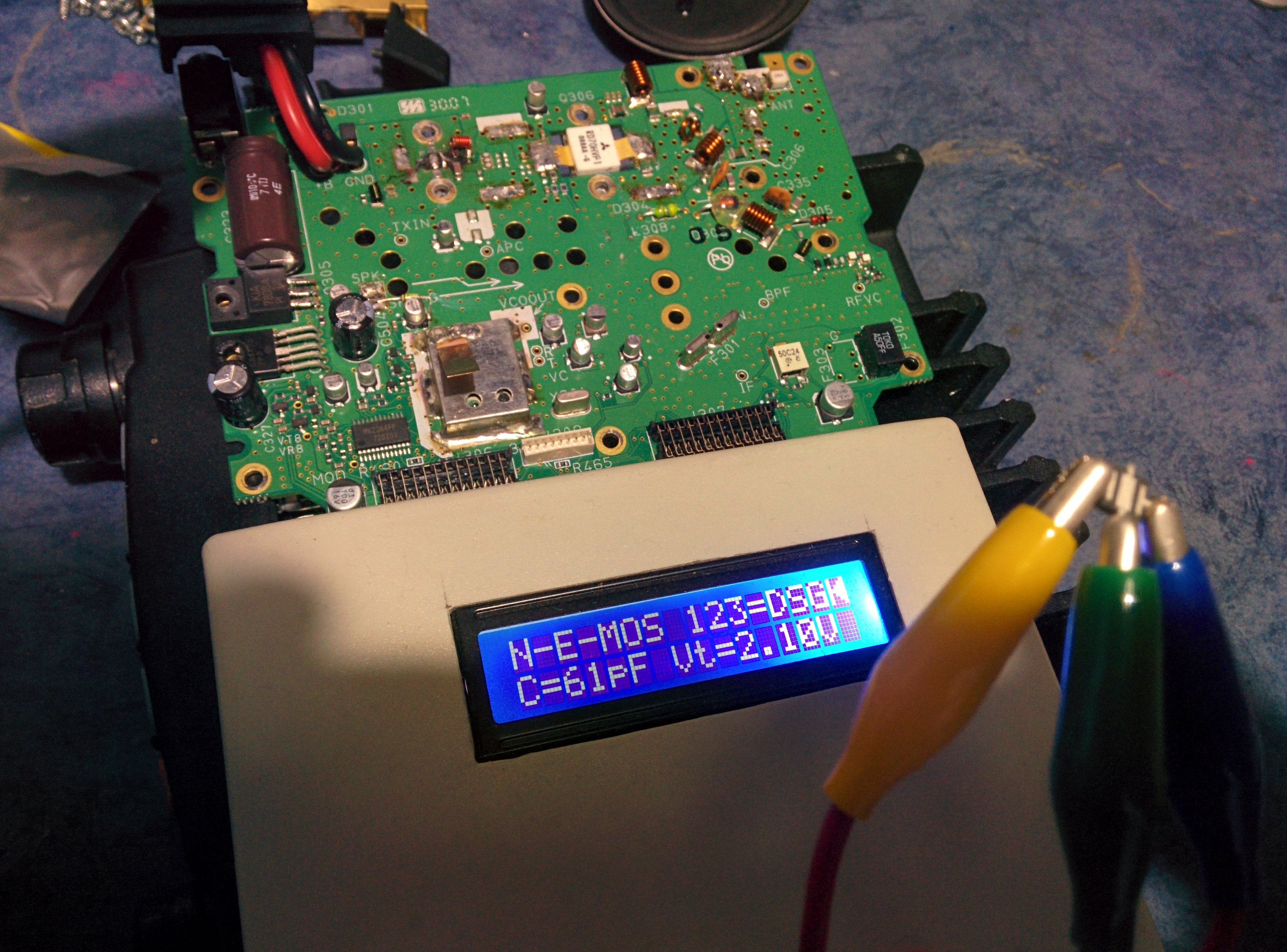
Before fitting the replacement, I thought I’d use a transistor tester to check the replacement part at least measured sensibly. Just before everyone emails me and tells me this isn’t how you check an RF part, I know, but it’s a crude test to see if it’s reasonable! A short circuit is still a short, an open is still an open. This seems reasonable!
From here, I cleaned the area up, removed the flux residue and then mounted the new part. This is extra complex too, because you need to make a good solder joint to the central pad on the heatsink/FET, since this is how the driver FET dissipates heat into the heatsink. Obviously, the soldering iron has its work cut out here, because the entire assembly is trying to stop the transistor getting hot. I packed around the copper heat-spreader with cotton wool to help it retain the heat. My 130W soldering iron was able to heat the central tab to a good temperature. I was then quickly able to clean the old solder away, and re-tin the heat-spreader pad. I then, carefully dropped the driver FET onto the slightly tinned heat-spreader in the correct orientation (refer to board silk), and the solder pulled and self aligned the part onto the pad. I rapidly soldered the remaining two ground connections, and then let the part cool somewhat before soldering the gate and drain.
As previously mentioned, I ruined the driver gate track, so I used a single strand of copper wire to the plate-through-hole on the board. This was slightly moved away from the ground pad, and I also had to bend the screening can a little more to create some relief for the extra jumper wire. I’m not proud of this, but it’s what I did:
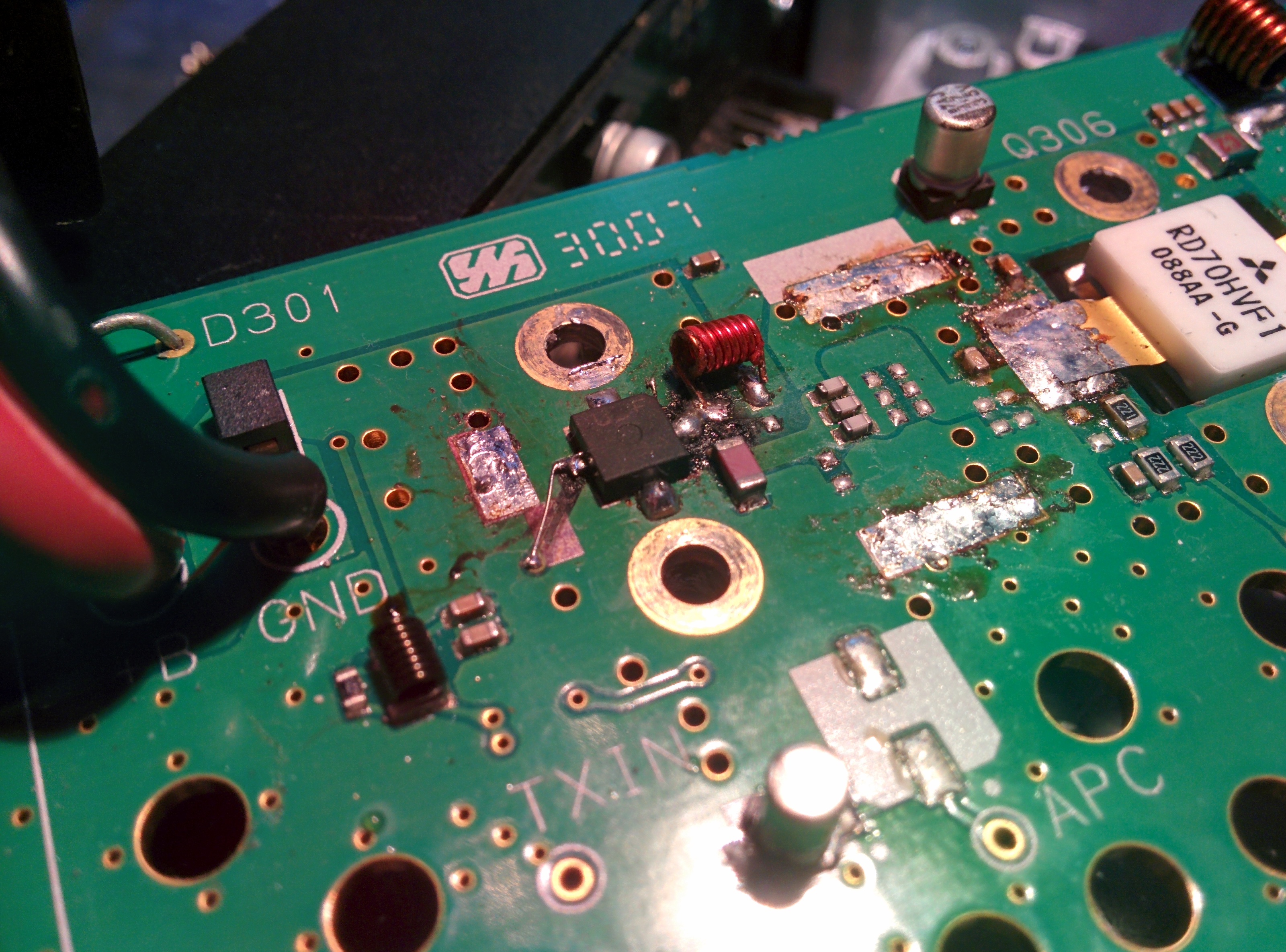
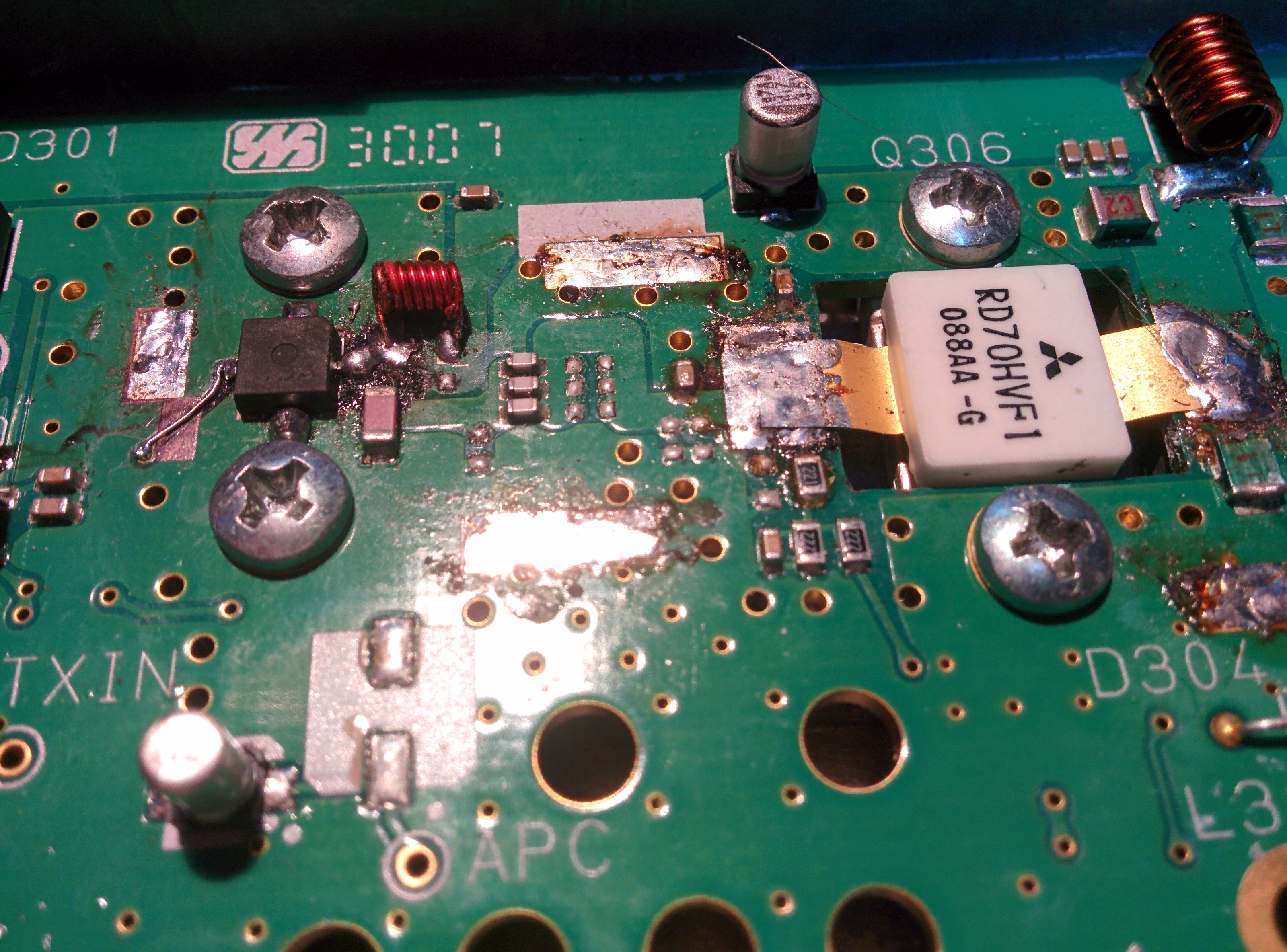
Finally, here’s what the whole PA strip looked like. Just cleaning up of the flux and re-wetting the main transistor joints to go, and we’re away!
And after the alignment, here’s the PA doing 65W again (approximately).
There you have it again. The third time I’ve worked on this radio’s PA!