Tag Archives: arduino micro

An easy-to-build interface for Morse Paddles & Keys…

I recommend Ham Radio Duo’s video on Morse Code Tools: CW Practice and Games (N4BKY & N4FFF) for a more detailed overview. Most of the tools here are covered in their video!

When learning CW there are many online practice tools:

  • Morse Invaders (KE6EEK) – a simple game for practicing sending morse in a space-invaders style – very addictive!
  • Morse Code AI Chat Bot (N4BKY & N4FFF) – an AI chatbot that sends and receives CW
  • V-Band () and Vail () – online ham-band platforms where you can practice CW with others
  • Morse Code Battleships (N4BKY & N4FFF) – an interactive battleships game with CW interface

I really also like MorseWalker (W6NCY), a joke on the contest practice software MorseRunner (VE3NEA). I really enjoy using MorseWalker – but it’s receive practice only.

For those that need CW paddle input, you really want to be using an interface – that way, you can connect your favourite key (or, failing that, the key that you’ll be using) to your computer and practice sending with that key…

Interfacing Options

There are a couple of existing interfaces:

  • The Vail Adapter is a full project with custom PCBs, etc., and works well.
  • The VBand Adapter can be purchased from their site.

Because I am impatient and had the parts, I decided to build my own.

The Build

I took inspiration from the OZ1JHM’s hamradio-solutions-vband-interface code. I am mainly interested in the paddle operation, but, you could modify this code easily to just send a single keyboard-button press for the straight key.

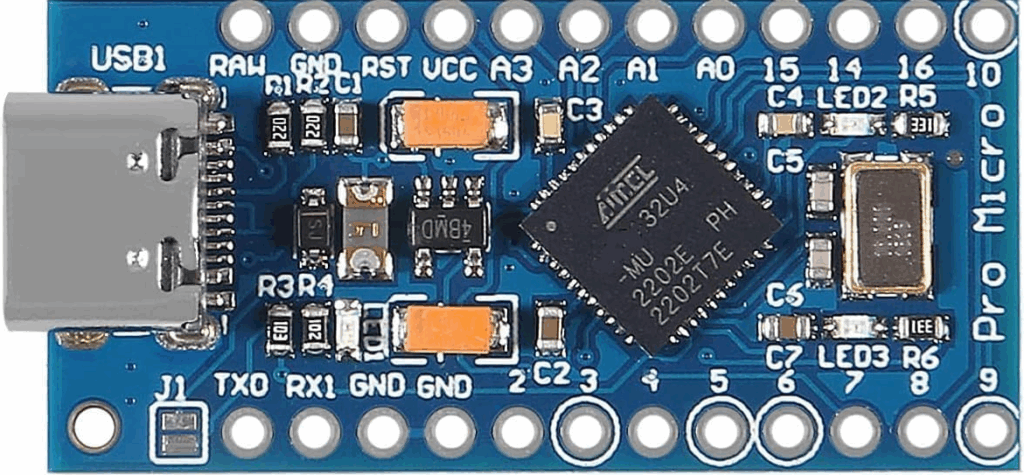
It’s important to note that you’ll need an Arduino where USB is directly connected to the Arduino chip and not via an UART IC since these only support UART ports and can’t emulate a keyboard. This means that you cannot use devices based around the Atmega328P.

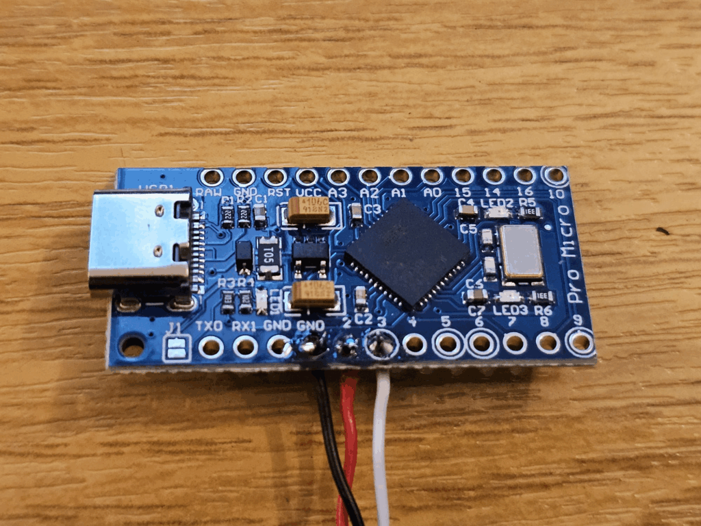
The code below is for an Arduino Pro Micro (I used a USB C version) which is based on the Atmega32U4:

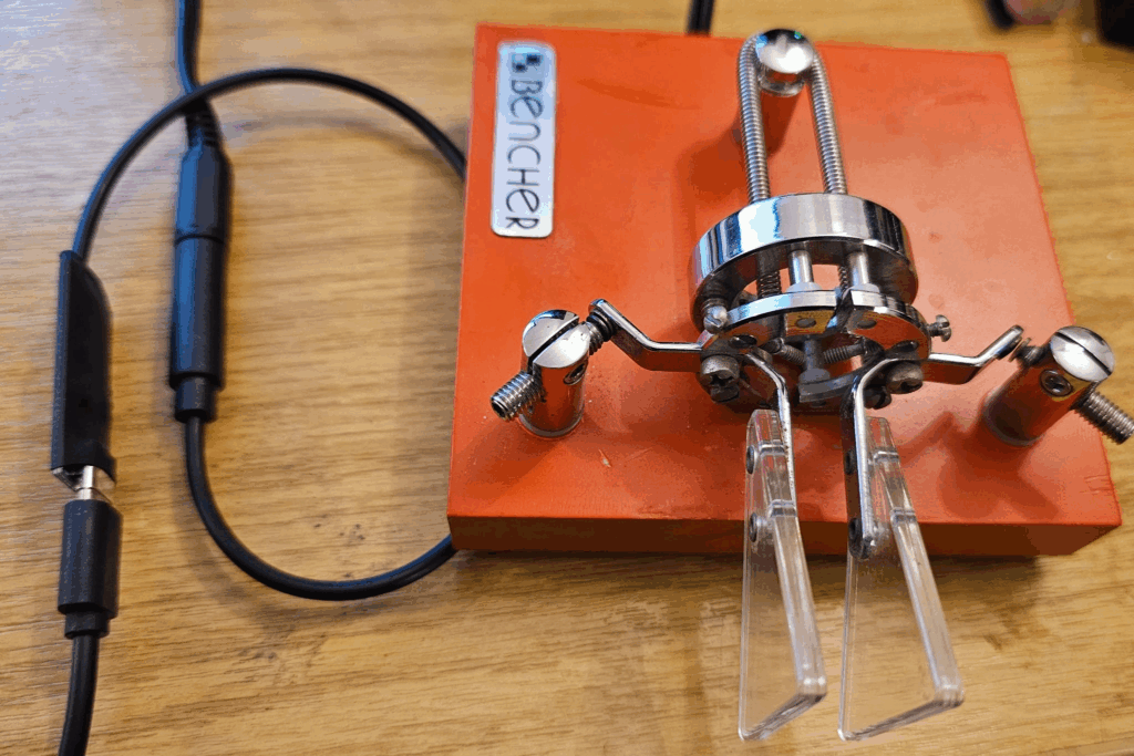
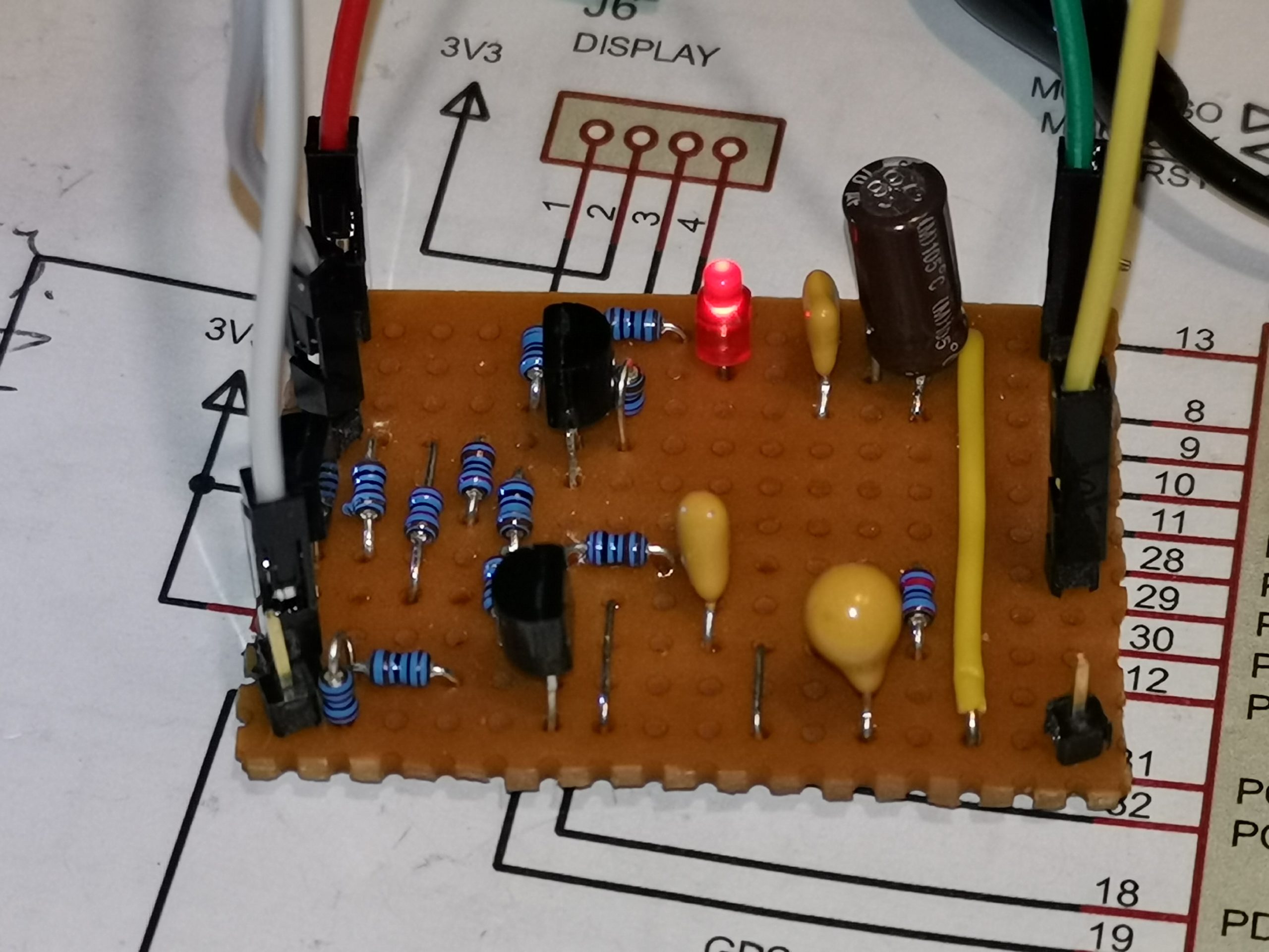
You’ll also need a way to connect your key easily. I used a moulded 3.5mm (1/8in) stereo socket on a short cable (available online cheaply) to create a nice connection, that would allow me to easily plug & unplug my key.

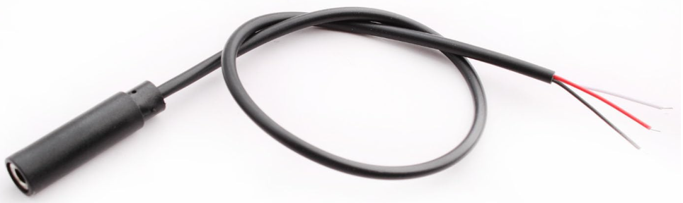
It is then fairly straightforward to make the 3 solder joints needed:

  • Black: GND
  • Red: A2 (dit)
  • White: A3 (dah)

You may have to tinker around with the connections a little bit to get your radio, the adapter and your key to work interchangeably. Above is what it ended up being for me.

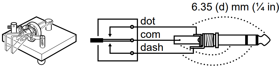
Above, taken from the manual of my Icom IC-7610. I have wired the Arduino to have the same polarity as the radio, assuming this to be the standard. Note, the radio uses a 6.35mm (1/4in) jack, not the smaller 3.5mm (1/8in) as we’re using.

And you’re ready to program the MCU! We’ll finish up with the hardware once we’ve checked it works!

Arduino Pro Micro Code

// Include the keyboard drivers
#include <Keyboard.h>

// Pin Definitions: Where the paddle pins connect.
// Note: Closing the contact should ground these pins.
# define DIT_PIN 2
# define DAH_PIN 3

// Arduino setup code
void setup() {
  pinMode(DIT_PIN, INPUT_PULLUP); // en internal pullup (dit)
  pinMode(DAH_PIN, INPUT_PULLUP); // en internal pullup (dah)
  Keyboard.begin(); // start keyboard runtime
}

void loop() {
  // While no paddle button is pressed, release all keys.
  while (digitalRead(DIT_PIN) == HIGH && digitalRead(DAH_PIN) == HIGH){
    Keyboard.releaseAll();
  }
  
  // On DIT pressed, send LEFT CONTROL key, else release
  if ( digitalRead(DIT_PIN) == LOW){
    Keyboard.press(KEY_LEFT_CTRL);
  } else{
    Keyboard.release(KEY_LEFT_CTRL);
  }
  
  // On DAH pressed, send RIGHT CONTROL key, else release
  if ( digitalRead(DAH_PIN) == LOW){
    Keyboard.press(KEY_RIGHT_CTRL);
  } else{
    Keyboard.release(KEY_RIGHT_CTRL);
  }
  
  // Wait 5ms
  delay(5);   
}

Tidying it up!

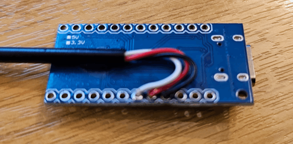
Once you’re happy it is working as you wish, an optional step for longevity is to protect the PCB. I did this by first applying a dot of super-glue to the cable and attaching it to the back of the PCB (note how I brought the wires out on that side).

Next I used some heatshrink tubing to cover the board, protecting everything.

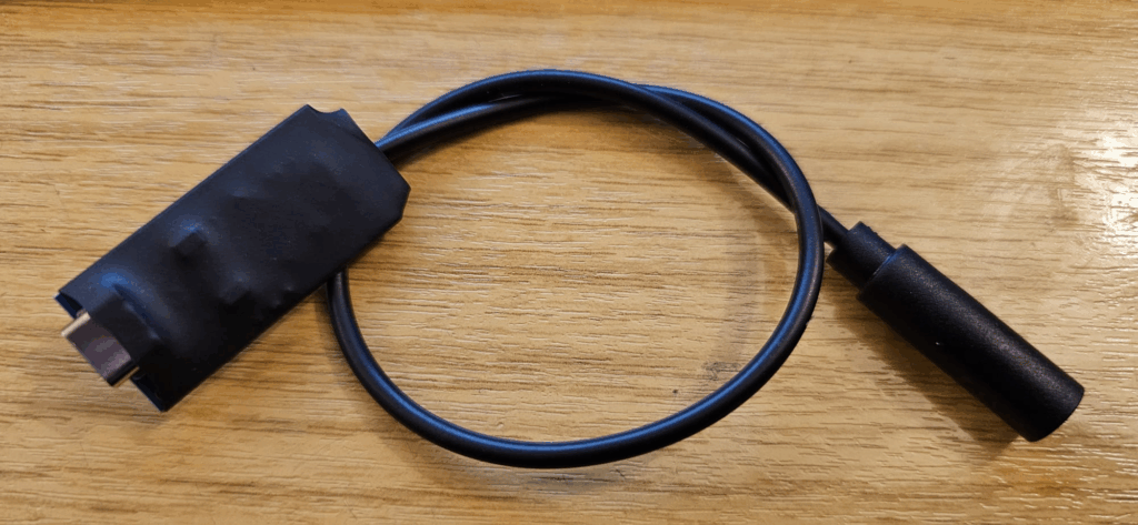
And, you’re good to go!

With that, you’re ready! Connect your key, connect your USB cable, and you can practice until you’re CW is perfect!

Experiments with Phase-Frequency Detectors

Over the past few evenings, I have been experimenting with phase-frequency detectors. I have an upcoming project that requires the use of one, and, I figured I’d refresh my memory on them. I ended up using my Lattice MachXO2 breakout board as the development platform.

The first step was to divide a 10 MHz crystal oscillator down to 10 kHz. That was easily done with a counter, counting from 0 to 499, and then resetting to 0. Every reset would simultaneously toggle an output bit, with the net result being a square-wave clock on the output bit, periodic every 1000 cycles of the input. A divide by 1000 counter.

Next was to understand the Phase-Frequency Detector (PFD). This is commonly referred to as a Type 2 detector, since it detects not only phase difference but frequency difference. This means that the PLL will only ever lock to the fundamental frequency, and not harmonics. It also means that when the loop is unlocked, the PFD knows which way to drive the VCO to regain lock. A Type 1 detector only uses phase information, and so drives the oscillator in the direction of the phase difference until the loop locks – as a result, Type 2 detectors lock quicker.

The Type 2 detector has two outputs, up and down, which pulse for the required direction with a duty cycle proportional to the phase difference.

I spent a few days designing and simulating the PFD using the Aldec Active-HDL simulator to confirm that my circuit did indeed perform as expected:

I then added a simple lock detector, which set a locked signal high if the phases were in lock for the past 10 cycles as a proof of concept. In reality, a much longer observation window will be used. It is possible to see the lock signal becomes high after 10 cycles.

The final stage of this project snippet was to test on real hardware. The Verilog code was pushed through synthesis, place and route, and a configuration file for the Lattice FPGA generated. This was then programmed into the board, and the board taken to the lab – you can see all the main parts of the setup in the photo below.

Below, you can see the scope traces from the probes in the lab bench photo. The yellow trace shows the 10 MHz VCO frequency from the Trimble 34310-T2 OCXO. The green trace is a debug from the FPGA output showing the 10 MHz signal divided down 10 kHz. The blue trace is GPS locked 10 kHz reference output. Finally, the purple is phase detector output, here from the ‘down’ output of the detector since we see that the divided VCO output (green) slightly leads the GPS reference (blue). The ‘up’ output is at logic-0 throughout.

The next part of the project was to create the charge pump circuit which converts the ‘up’ and ‘down’ pulsed signals into an analogue control voltage for the VCO.

The parts for the charge pump took a few days to arrive, and while waiting I contrived the following circuit. Since the OCXO generates a 6V reference voltage for use with the VCO input (actually 5.4V in my case), it seemed wise to use that. Some crude experiments had lead me to a tune voltage of around 3.5V. The circuit uses a PNP transistor (Q1) to put pulses of energy into the filter network via R1. Similarly, it uses an NPN transistor (Q2) to remove pulses of energy from the filter via R1. R5 and R6 serve as a current limit in case both Q1 and Q2 are both powered. A further NPN transistor (Q3) acts as a voltage interface between the ~6V on the base of Q1 and the FPGA IO at 3V3 maximum. Only the values of components in the filter section are critical (R1, R7, C1, C2, C3); the others were chosen from what I had laying around.

The loop filter was tested and tweaked in LTspice using the values above. The loop filter has around 62 dB of attenuation at 10 kHz (our reference [and thus up/down pulse] frequency).

A look in the time domain shows we can expect about 1.5mVp-p at 10 kHz from visual estimation. An output of 1.5mVp-p is approximately 0.53 mVrms, which gives us around -66 dBV of attenuation (similar to we saw above). The curve of the waveform is the DC levels settling out at the start of the simulation.

And finally the steady-state ripple; for a 1V square wave (0V-1V) input, a 1.23 mV ripple exists at the output (455.719-454.486).

The penultimate step was to build the circuit and confirm it worked in real life. I made the charge pump on a scrap of strip-board, with pin headers for the main signals. On the left, +6V VCO reference input, the up and down signals from the FPGA, and on the right, ground and the VCO tuning input. The circuit is pretty much laid out as per the schematic, with the addition of an LED.

The final step was to watch the PLL lock on the scope! In the short video clip below, you can see the yellow trace is the 10 kHz reference frequency from the GPS. The green trace is the 10 MHz from the VCO. The blue trace is the 10 MHz divided down to 10 kHz. The purple trace is the VCO tune voltage – the output of the charge pump.

The closing remark is that this project was a learning exercise. The Verilog code & TB is presented here on GitHub and you’re invited to take a look.