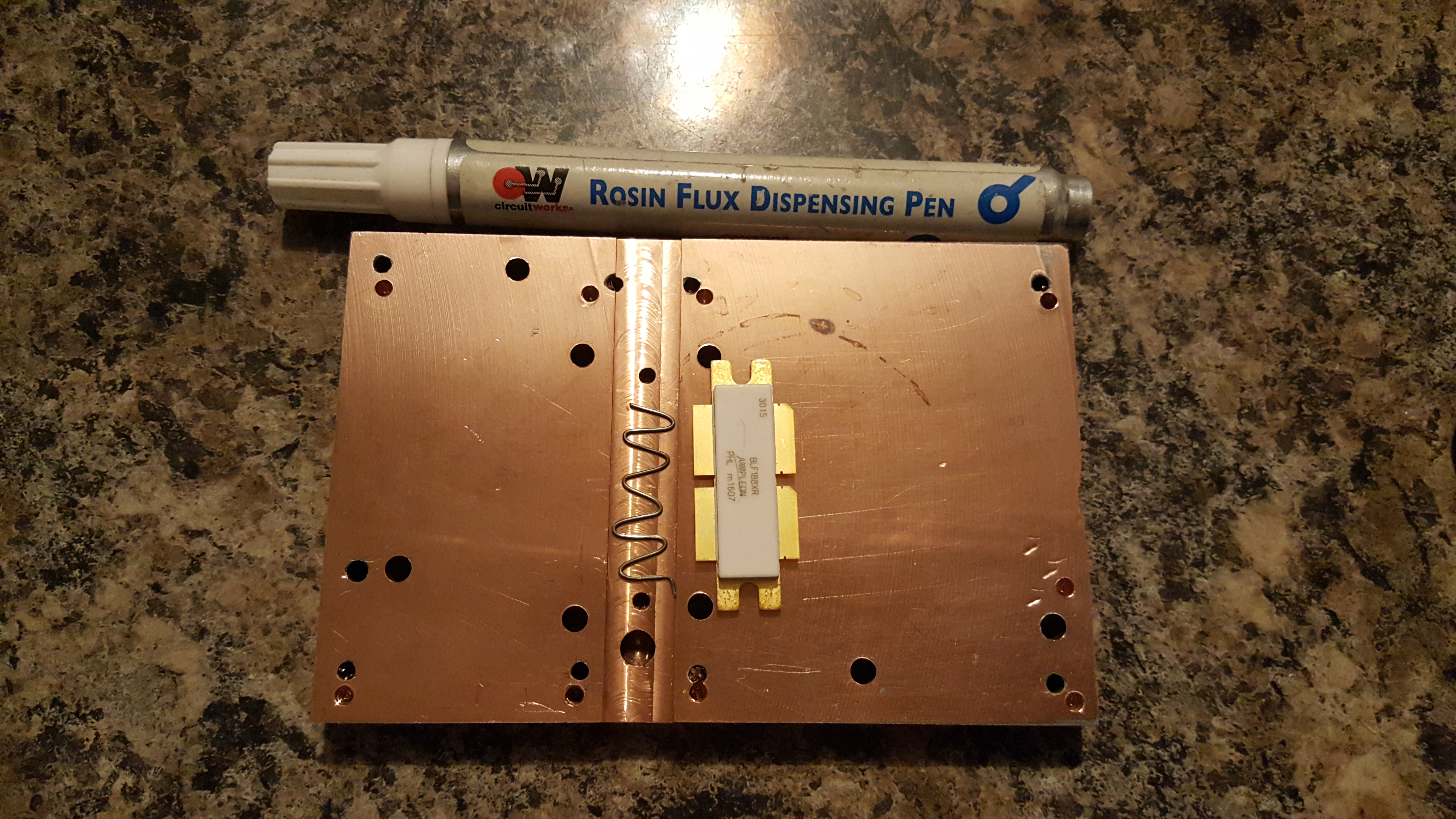
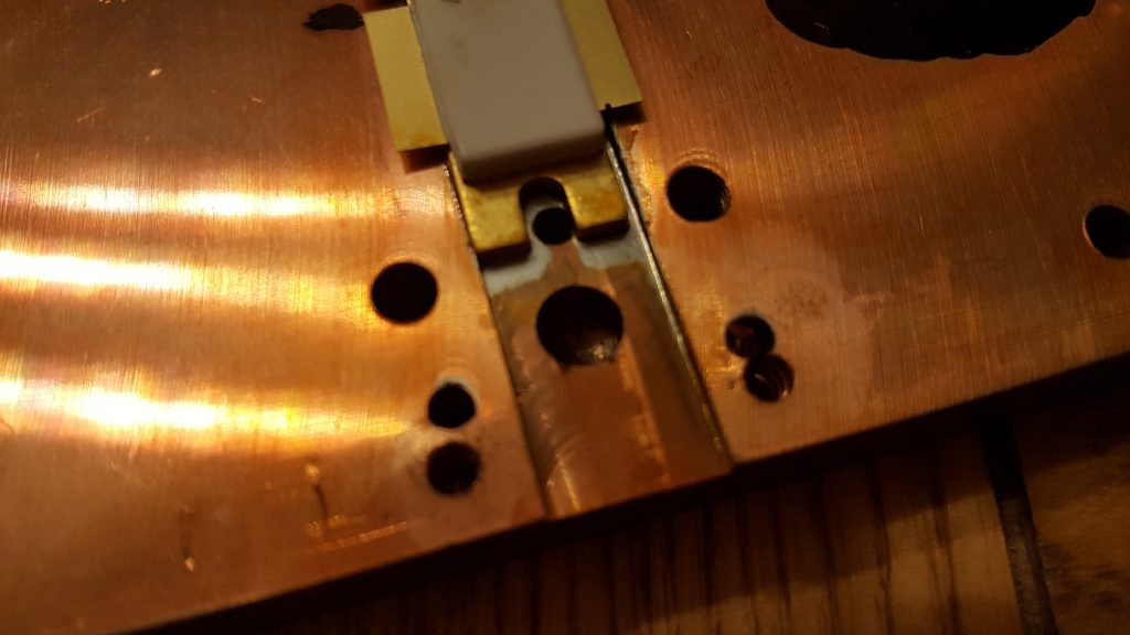
This morning, Royal Mail delivered me a parcel from Jim W6PQL all the way from California, USA. It took a couple of days to clear customs, but it arrived within about 5 days of being ordered. If you followed my previous post on this subject, about machining heatsinks, you’ll know that the last transistor I had failed on the testbench. You’ll also know that the copper heat-spreader was re-machined to suit the new PCB. This is why the heat-spreader has a few extra holes. Seeking advice from veteran microwave DXers & constructor (G4BAO, G4DDK, G8KBV, et al.) I was instructed to solder the device down. I watched a few of Jim W6PQL’s videos on soldering LDMOS parts to the copper heat-spreaders and replicated his instruction as closely as possible. You can see Jim’s instruction video here.
A small length of thin leaded 60/40 solder was made into a wiggle for the length of the transistor and placed in the groove previously machined in the head-spreader. I liberally applied flux to the bottom of the groove and the underside of the transistor and then sandwiched the solder in between.

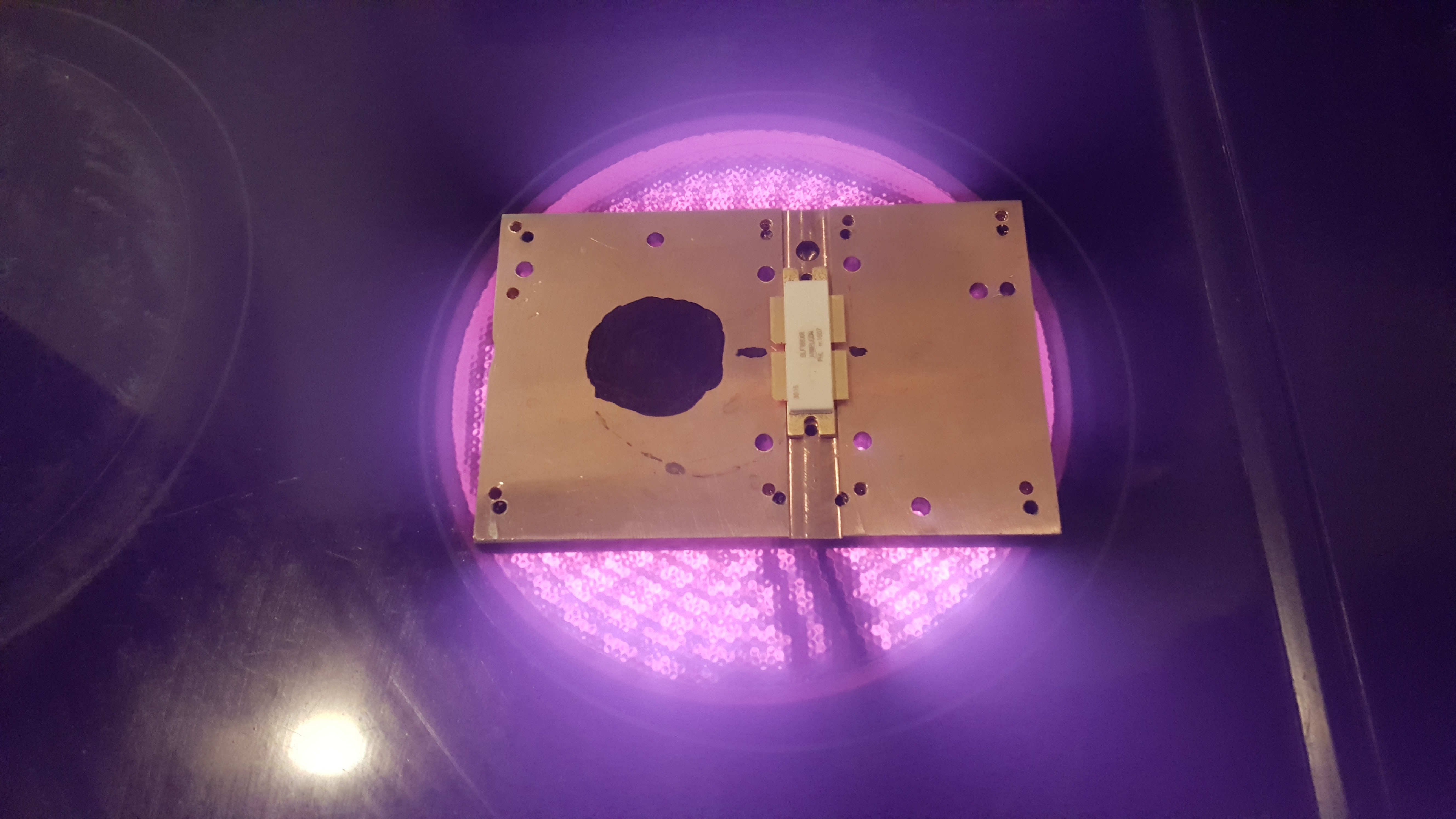
The copper heat-spreader was placed on the electric infrared hotplate and heat applied. The black dot is used to allow a laser thermometer to monitor the copper temperature. NB: this method didn’t work well.

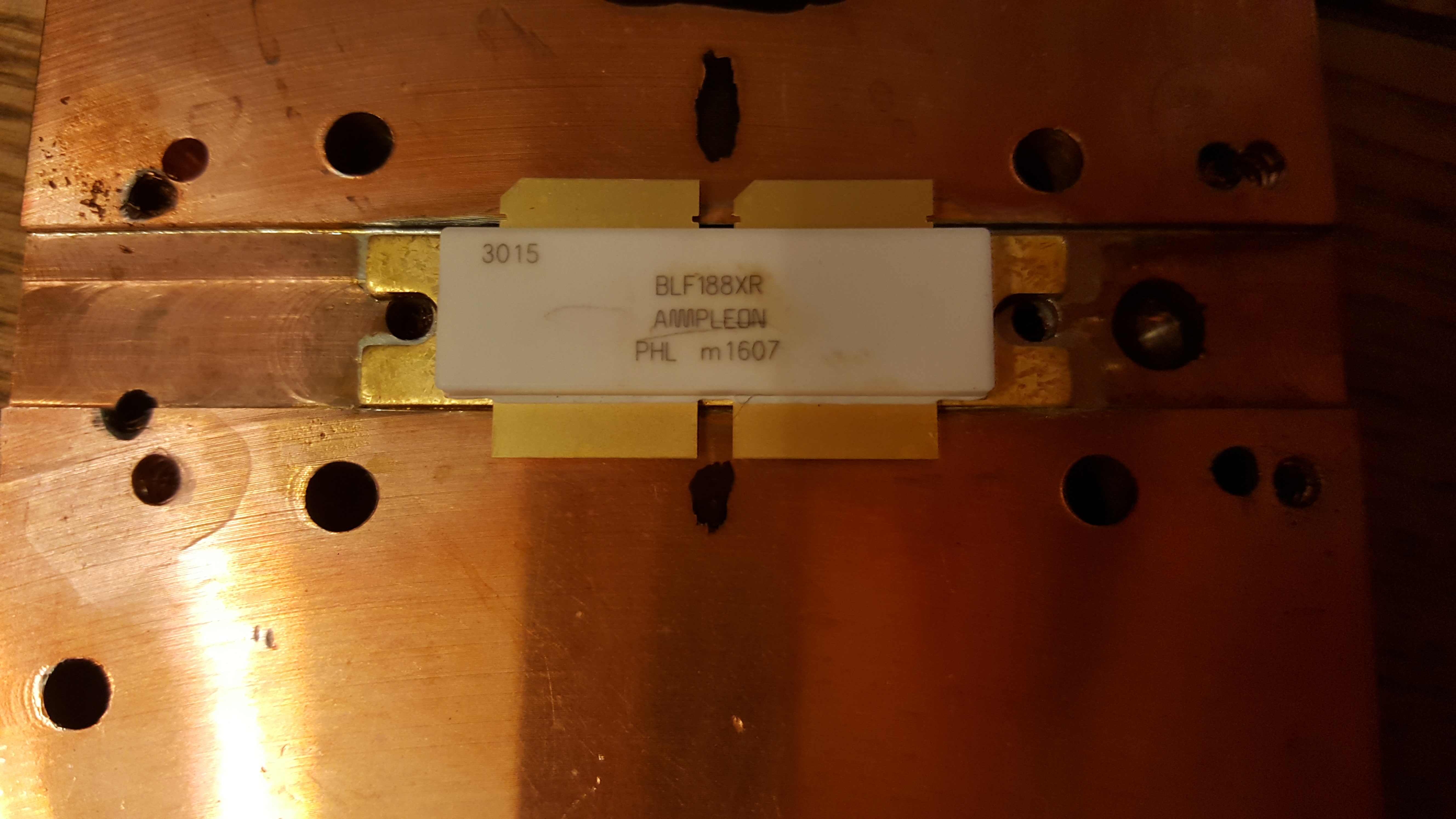
The next two images show the solder has melted and the excess squidged out the sides. It’s clear to see when the solder has melted, since the the transistor drops. It is advised to move/slide the transistor in the molten solder to remove any voids and any excess solder. I immediately killed the heat and removed the spreader from the hotplate and placed it on a heatsink. It only took a couple of minutes to cool to a temperature I could handle, and I checked the location of the transistor against the PCB mounting holes.

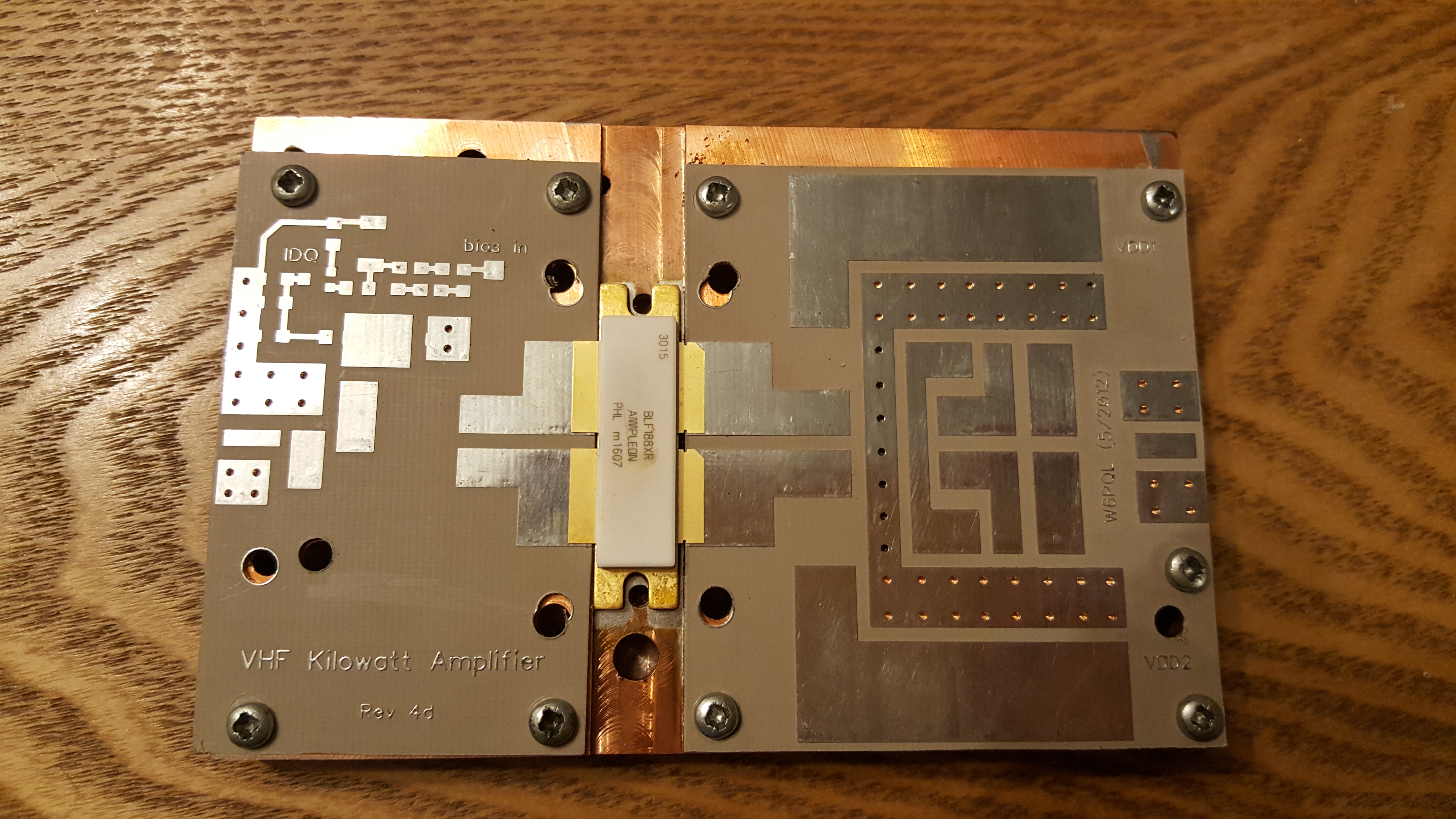
The PCBs were finally mounted as a test fit. I will populate the boards before mounting them. Unlike the original jrd1 boards, these PCBs do not need to be soldered down. This means the boards can be soldered up and then mounted.

Stay tuned for more updates…

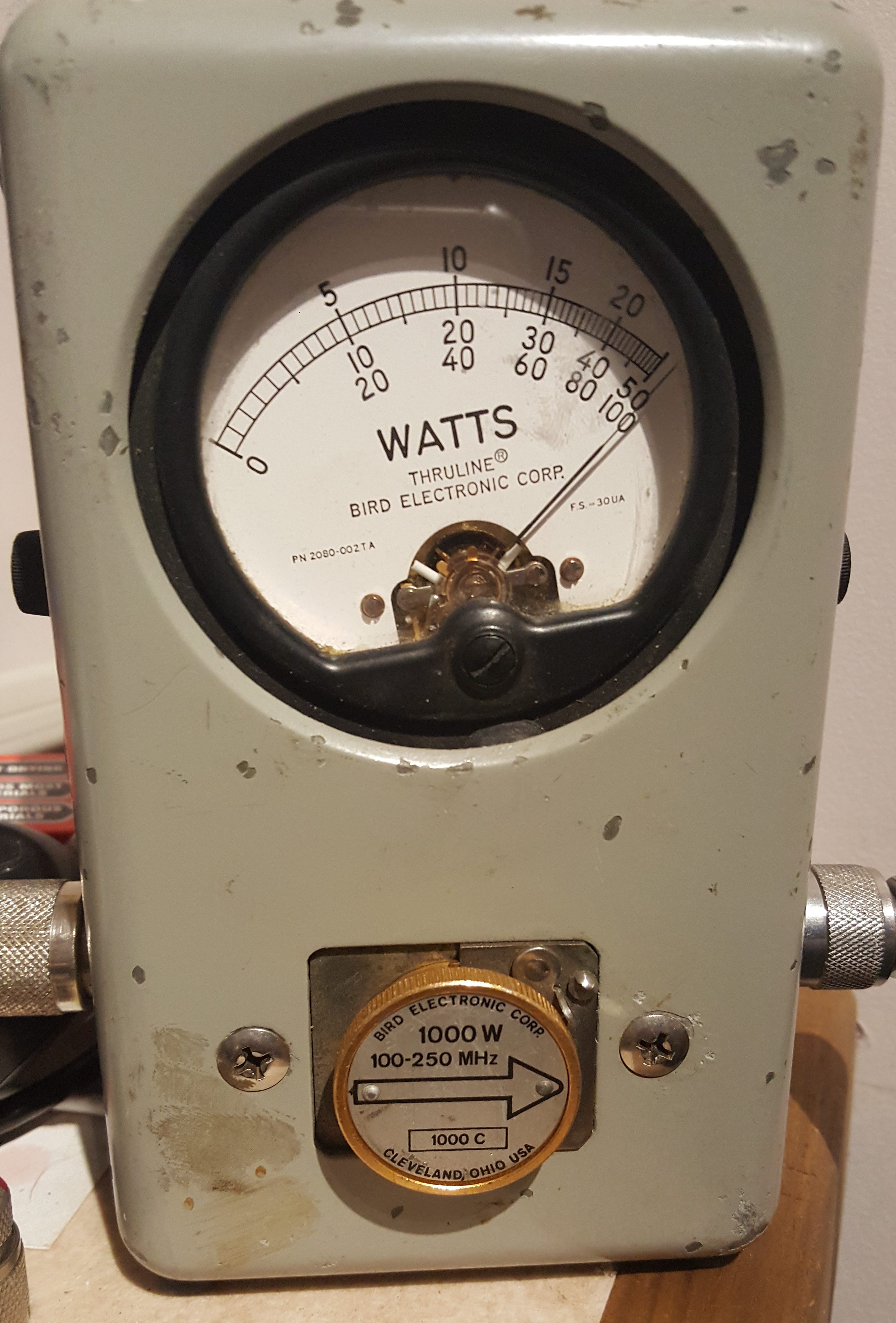 The amplifier was able to maintain in excess of 1000W for over 2 minutes. At this point, the Bird dummy-load started to get a bit warm, so a longer test was abandoned. The amplifier pallet, however, remained cool enough to touch. As the F1JRD original design notes, the 10-Ohm coax balun does become hot (Lionel suggests around 120C at 1kW with no cooling). I, however, used a small fan running slowly to provide a gentle draft which greatly reduced the balun heat.
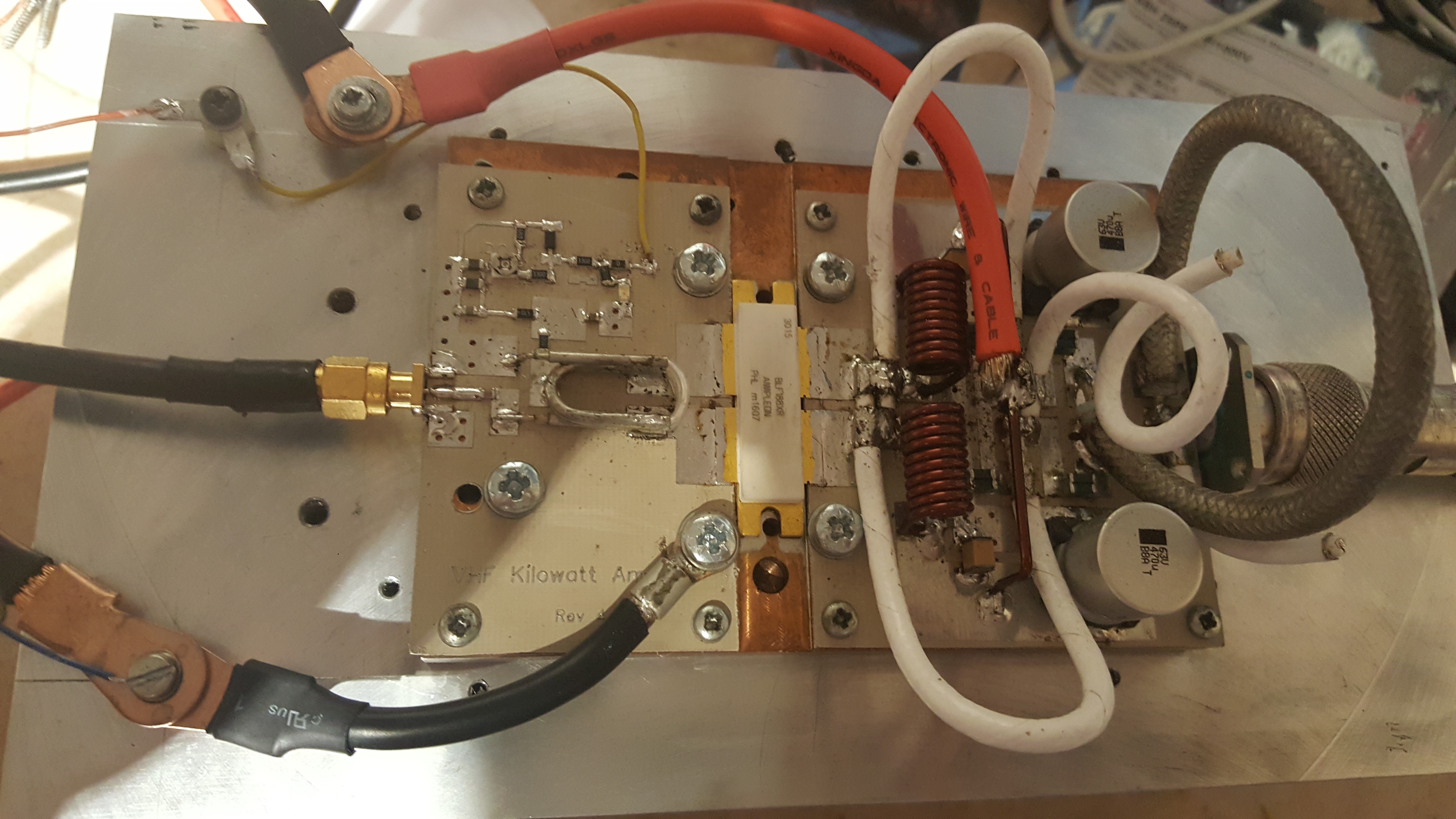 The next step is to add the Dallas-Maxim DS18B20 temperature sensor – the idea is to have the sensor buried into the pallet next to the transistor, to measure the copper heat spreader temperature.