This page is about the Chinese RF_PA_250_3_HV_V201 by ZGJ 2018-01-25, version 201, commonly for sale on eBay, AliExpress, etc.
Sellers, you are welcome to link to this page in your listings.
This page is a mix of information from my own investigation as well as information found online (from several sources). It is useful for those purchasing kits for such amplifiers.
Bill of Materials
| Reference | Quantity | Part |
| C1, C2, C8, C11, C19, C20, C21, C22, C24, C25, C26 | 11 | 10nF (103) |
| C3, C9, C10, C13, C15, C16, C18, C46 | 8 | 100nF (104) |
| R29 | 1 | 10KΩ |
| R9, R10, R11, R12 | 4 | 5.6Ω |
| C5, C12 | 2 | 680pF Mica capacitor |
| C47 | 1 | 100uF 25V |
| C7, C14 | 2 | 1000uF 16V |
| L4, L5 | 2 | 220uH Color ring inductance |
| D9 | 1 | Red 2.54mm LED |
| D10 | 1 | 9.1V Zener diode (use with 24V power supply) |
| R30 | 1 | 560Ω 3W (use with 24V power supply) |
| R7, R8 | 2 | 220Ω 3W Power resistance |
| 1 | 20Ω 3W Power resistance | |
| RV1, RV2 | 2 | 5KΩ or 10KΩ preset pot |
| L1 | 1 | 13mm NXO100 magnetism ring (2 cores) |
| T1 | 1 | 13×5 NXO magnetism ring |
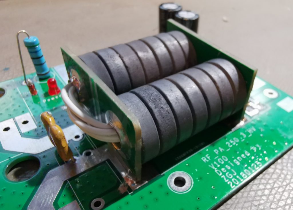
| T2 | 1 | Copper pipe 2pcs, 0.75 square mm wire (60cm long), 18mm NXO magnetism rings (14 cores) |
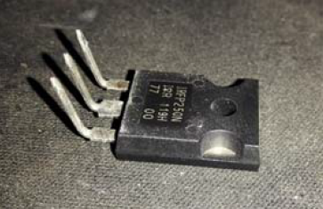
| Q1, Q3 | 2 | IRFP250 |
| U1 | 1 | LM78L06 or LM78L09 |
| Insulating spacers | 2 | |
| 0.8mm enameled wire | 1 | |
| 0.75mm high temperature cable | 1 |
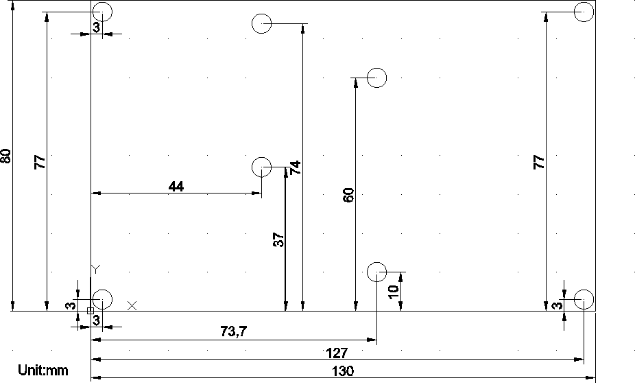
PCB Dimensions
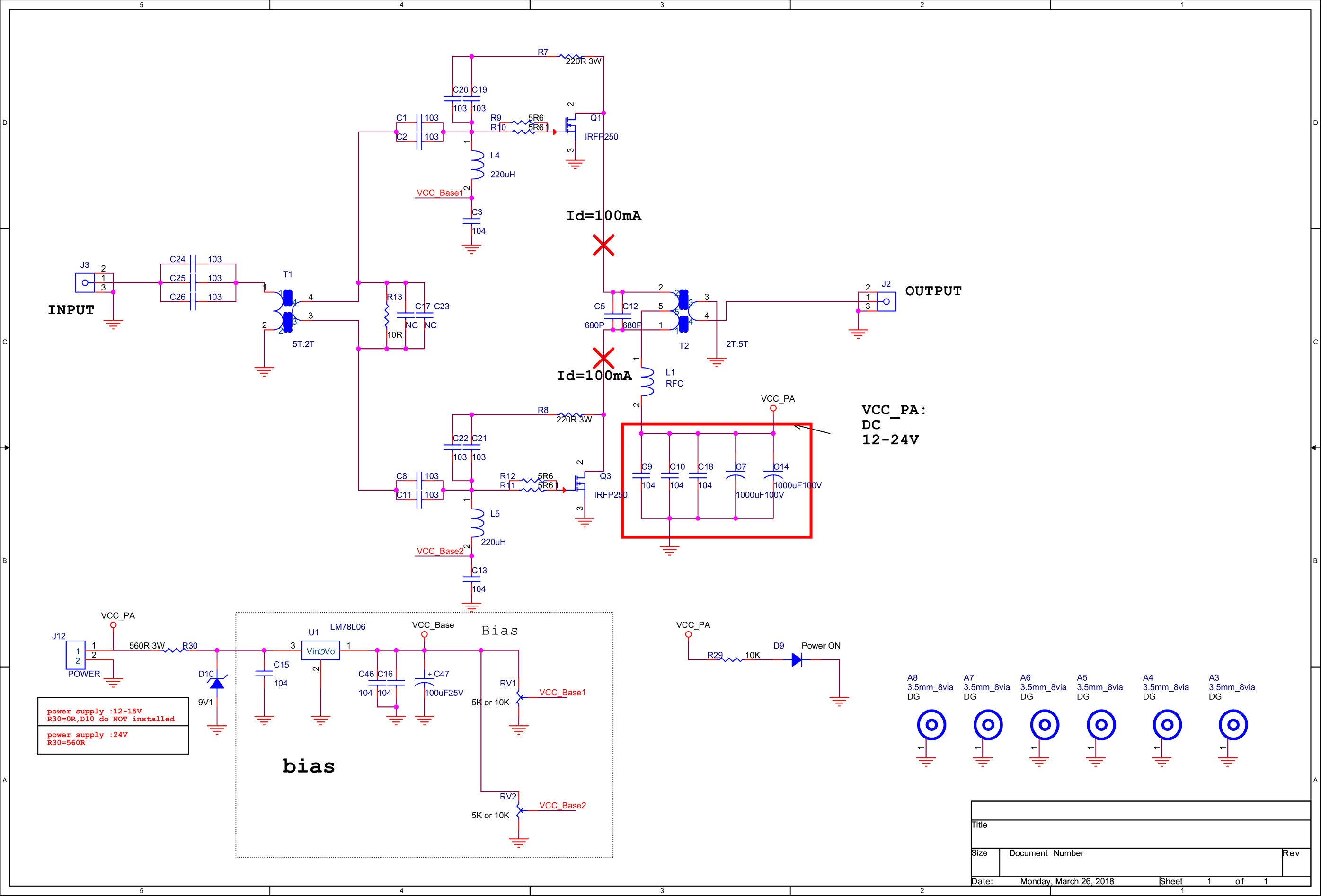
Schematic
Click image to enlarge. For transformer winding information, see below.
Build Information
Version History
- V100 – First edition
- V101 – Second edition: Output transformer cores reduced to 14.
- V201 – Third edition: Power supply voltage is raised to 24V.
What you will need
- 13.8V/24V 40A (or higher) power supply. It is better to have the function of current‐limiting protection. 6 square-mm (or more) wires for connecting the power to the amplifier board.
- A signal source that is capable of outputting a 7 or 14 MHz signal at 10W.
- A 50Ω dummy load rated for 200W (must be able to withstand continuous dissipation).
- A heatsink suitable to dissipate the power of Q1 and Q3. (Recommended size: no less than 150x100x60mm).
- A multi-meter that includes a 10A scale.
- An oscilloscope capable of at least 20 MHz (or a spectrum analyser).
Before you start soldering
- Wind the inductor (L1) and transformers (T1 and T2) in accordance with the information further on in this page.
- Bend the legs on Q1 and Q3 (TO247 package) upwards, see the illustration below. Do not mount it to the top side of the board. Do not shorten the leads.
- Tap the holes for Q1 and Q3. Screw should be M3 (3mm screw). Clean the heatsink, and remove any metal chips to avoid a short circuit.
Soldering
- Start with smaller components first, working up towards larger components and finally plugs.
- SMT parts can be easily soldered with an iron by adding a small amount of solder to one pad, and using tweezers to push the SMT part into the molten solder on the pad. Once cooled, add a small amount of solder to the other pads.
- L1 and C5/C12 are not fitted at this stage.
Preparation for Powering
- Check for any solder splashes, and poor or missing solder joints.
- Check the DC power supply resistance to ground – no short circuits. If you have not fitted L1 yet, test from the other side of L1 pad.
- Check the LM78L06 regulator output resistance to ground – no short circuits.
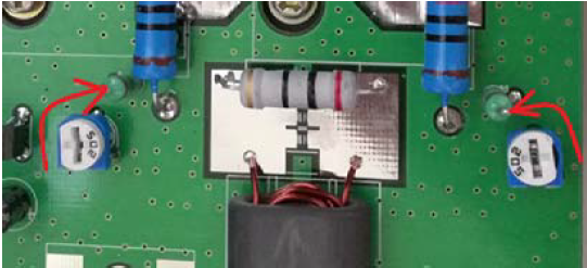
- Check the bias-set variable resistors. Rotate them as shown in the following diagram. Be careful, to rotate them to the correct end-stop. If you get this wrong, you will destroy the IRFP250N power MOSFETs. You are aiming for an initial bias voltage of 0V.
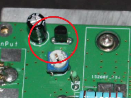
- Mount the input transformer secondary load resistor (10Ω, 3W).
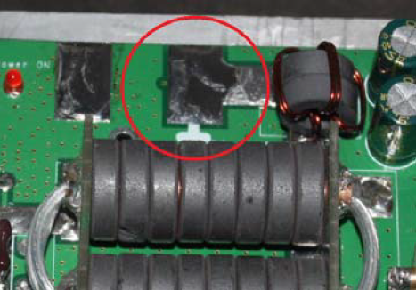
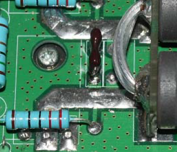
- Solder in Q1 and Q3 and affix to the heatsink. Flow solder on the PCB trace between the MOSFET and the output transformer. This increases the current capacity of the track. See below.
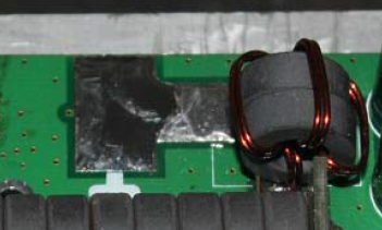
- Mount L1 as shown below.
Set bias currents
The aim of this section is to adjust the bias current to 100mA for each of the two transistors. When making adjustments, you must act slowly, and with great care – the current will do nothing for much of the adjustment range and then rise sharply. The transistors must be bolted to a heatsink during adjustment.
- Double-check that the variable resistors are ‘zeroed’ as described above, such that when power is initially applied, there is no bias voltage present.
- Connect a current meter in series with the positive power supply cable of the amplifier. Apply power.
- Adjust the upper MOSFET quiescent (static) current using the upper variable resistor to cause an increase in current of 100mA (0.1A).
- As before, now adjust the quiescent current of the lower MOSFET to further increase the current another 100mA. (A total increase of 200mA between both transistors.)
- Solder in choke inductor L1 and mica capacitor C5/C12 if you have not already done so – the bias adjustment is complete.
Signal test
- Connect a 50Ω dummy load to J2. The load must be capable of handling 200W.
- Use an oscilloscope on a suitable range (or spectrum analyser with suitable attenuation) to monitor the signal at the load.
- Connect the power supply and monitor the supply current for a moment. If the current is gradually increasing, the power must be cut immediately and check for suitable thermal connection between the power transistors Q1 and Q3 and the heatsink.
- With the amplifier powered and no input, check the oscilloscope for signals. If there signals, immediately power off and debug the cause of self oscillation.
- Input a small signal, gradually increasing the input signal power.
- Observe the output waveform and the DC input current. In general, 100Vpp output across the output load corresponds to a power output of 25W into 50Ω. A load voltage of 141Vpp is 50W output, 180Vpp load voltage gives an output power of 80W, and 200Vpp at the load is a power output of 100W. Using an efficiency of 55% as an approximation, the expected DC power input can be calculated.
- Check the temperature of the heatsink. If it is too hot to hold, then you will need to use a fan to cool the amplifier.
- Check the output power is stable over time, and that there are no large fluctuations in output power for a fixed input power.
Finishing
- Use a flux remover to clean any solder flux residue and tidy any poor solder joints.
- Mount the amplifier into a box or case with suitable TX/RX switching.
- Accompany the amplifier with a suitable low-pass filter board.
Transformer & Coil Winding
In the following diagrams process, please note:
- To avoid scraping the enamelled wire, use needle nose pliers to smooth the edge of the ferrites. Hole edges may be sharp.
- A “turn” on the coil is regarded as wire passing through the centre.
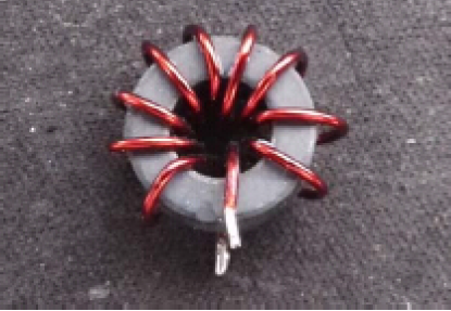
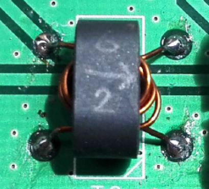
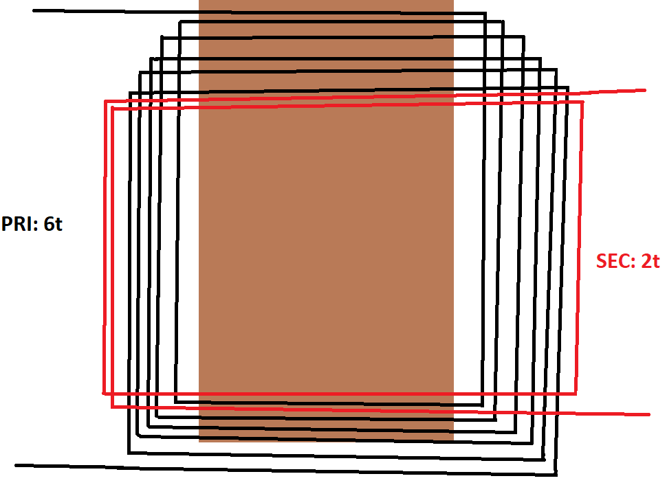
Winding T1
Transformer T1 primary should be 6 turns (black lines). The secondary of T1 should be 2 turns (red lines). The turns ratio is important, since if there are too many turns, the voltage on the gates of the MOSFETs will exceed the breakdown voltage and the parts will be destroyed.
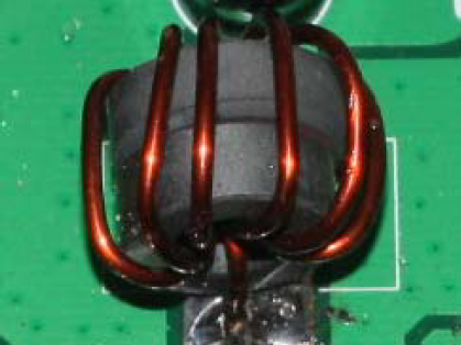
Winding T2
Transformer T2 primary should be 1 turn made from the two end PCBs and copper pipe. The secondary of T2 should be 5 turns of high temperature wire.
In version 201 of the kit, the number of ferrite rings is reduced from 16 to 14. You will also need 2 ferrites for winding L1 (see below).
Winding L1
L1 is a high frequency RFC choke. The 7-10 turns should be wound around two ferrite rings as used in T2. I chose 10 turns as this provides the largest choke inductance.