
I recently bought a cheap Qi Charger for my Google Nexus 5 phone from eBay. Other than that it met the Qi standard, I could never really find out what that meant. I appreciated that it was some kind of inductive charger system where a coil of wire in the charger couples to a coil of wire in the phone like the two separate windings of a transformer. However, beyond that, I was clueless. The Wikipedia artcile was kind of sketchy on the technicalities of the scheme: Qi (inductive power standard).
I decided to see what was going inside. I took the cover off to find that the device was mostly empty space. A small circuit board scattered with a couple of ICs and a coil of wire on a ferrite block is all I found.
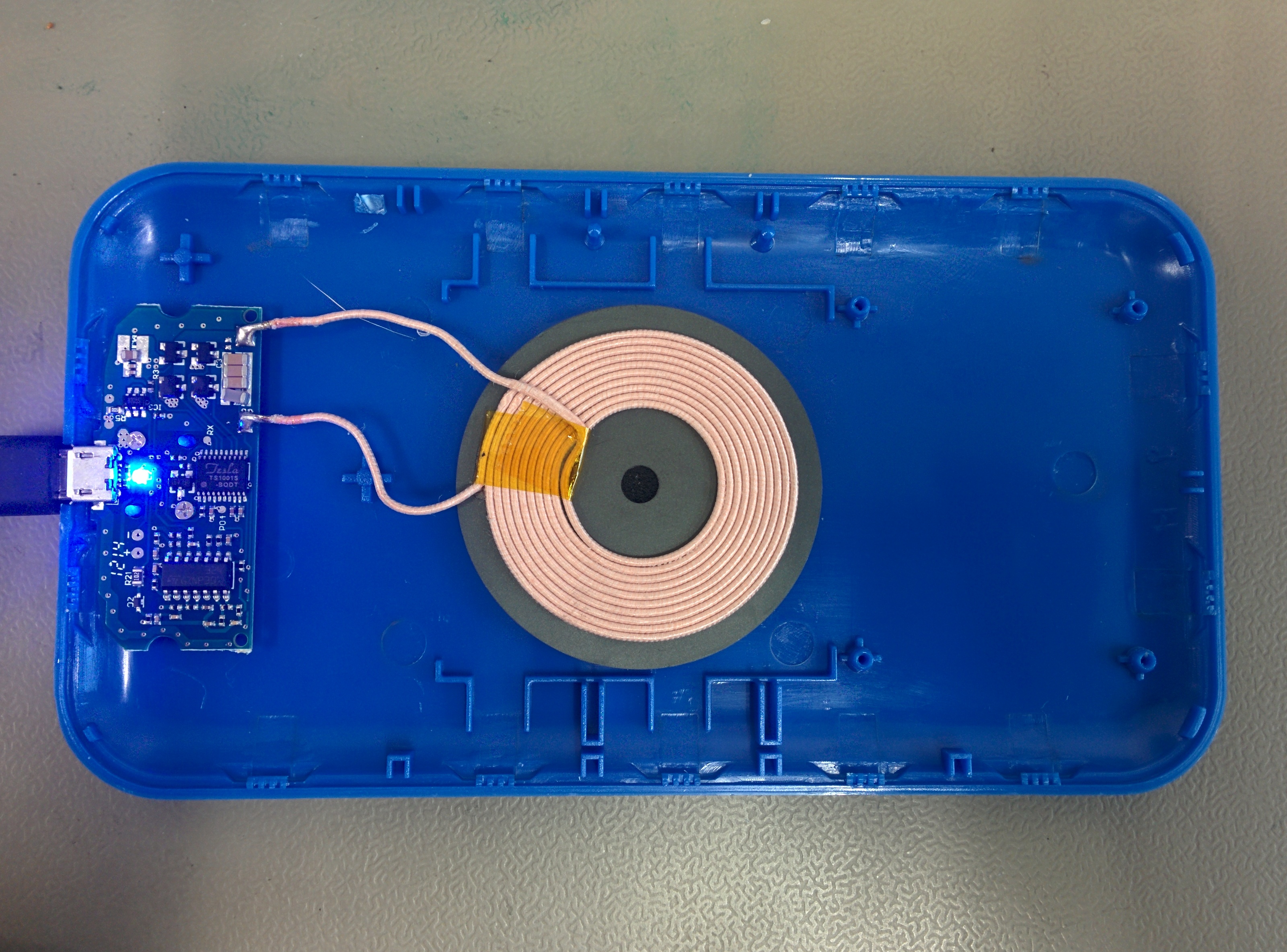
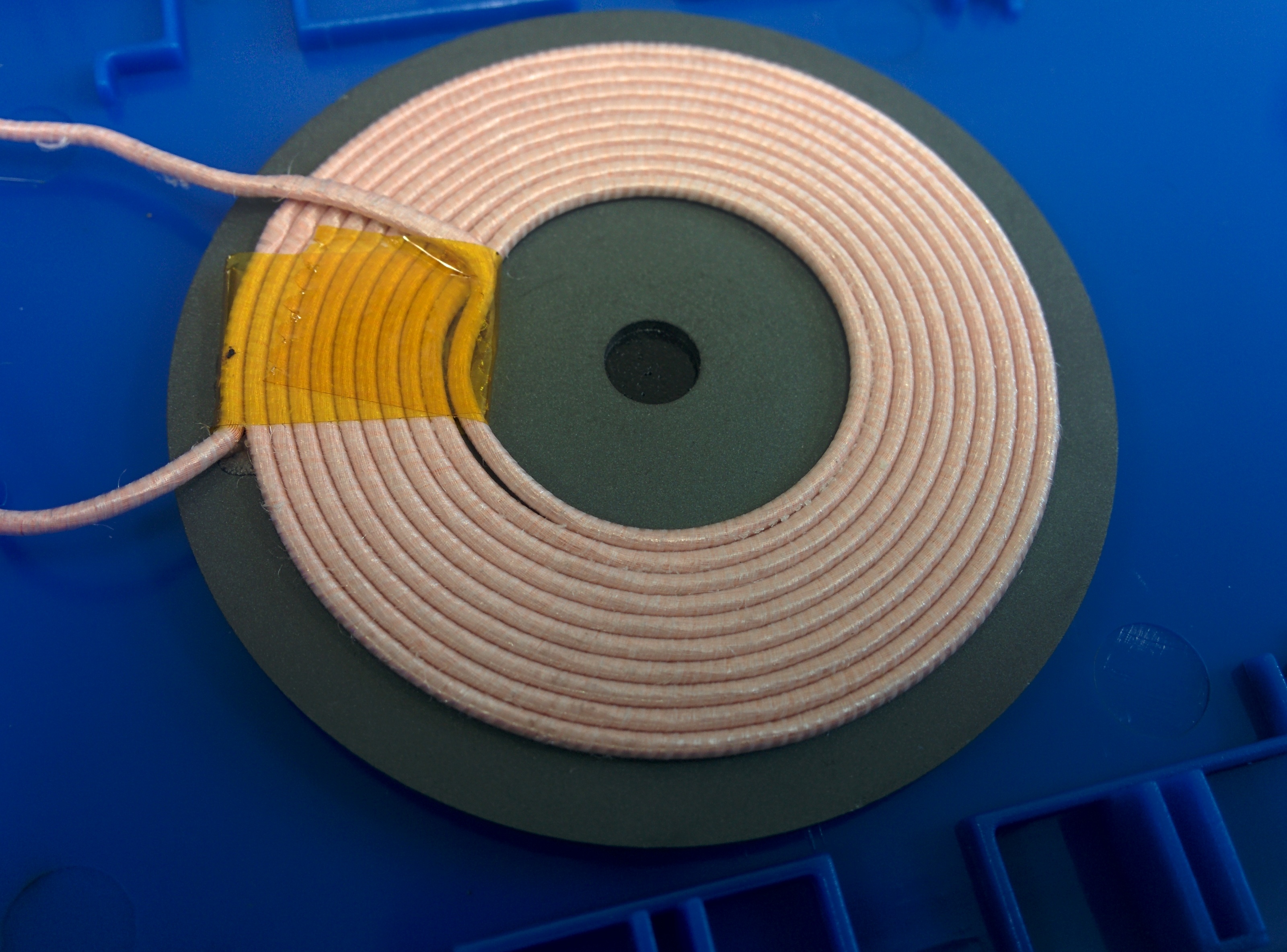
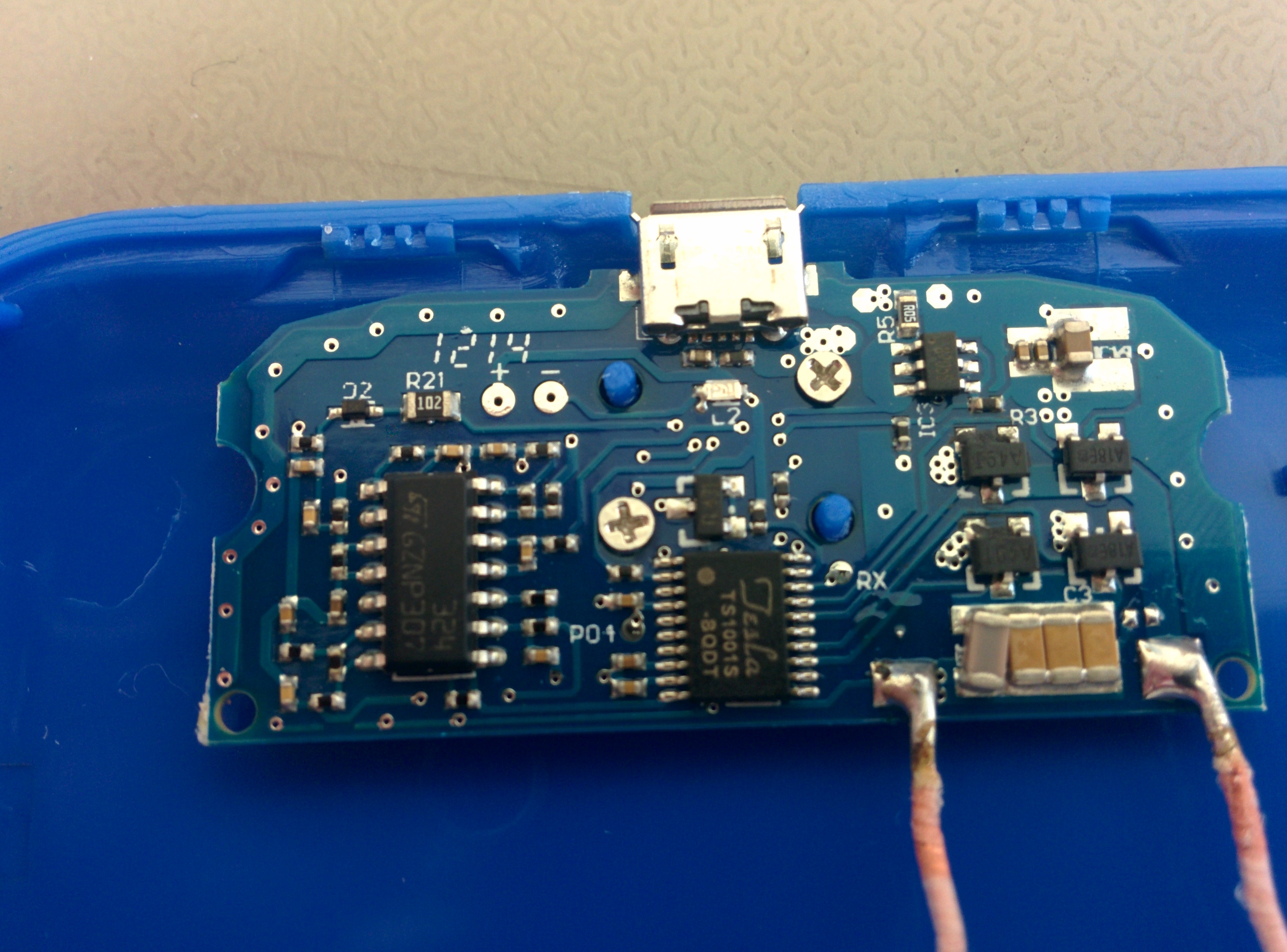
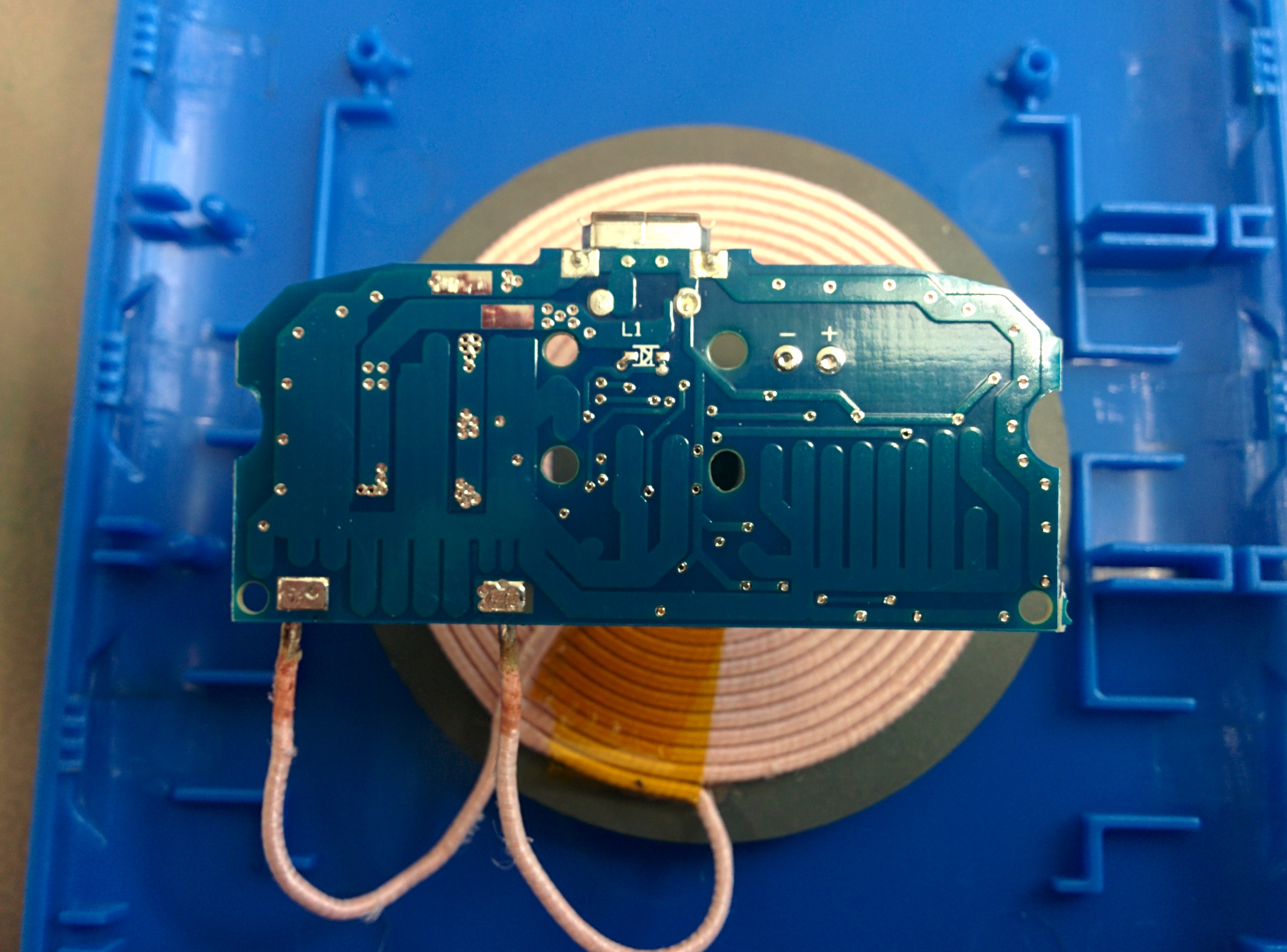
A close-up of the coil and both sides of the PCB
 |
 |
 |
Clicking on any of the pictures will load the picture details page. Click on the picture there, and it will show full resolution.
Looking at the middle picture (the top side of the PCB) you can see where the coil connects to the PCB. Between these two connections, 4 capacitors are used in order to get the coil to resonate on frequency. Looking around the net, figures in the region of 200 kHz are mentioned. This is also the purpose for the ferrite (grey material) underneath (see ferrite material and ferrite cores.
Above these capacitors, you see black surface-mount transistors. These are configured in a H-bridge configuration, allowing for a greater peak-to-peak voltage swing across the coil, and therefore more power. From here on there are some components that measure the current being drawn by the H-bridge (and thus the phone being charged) and some components that drive the H-bridge.
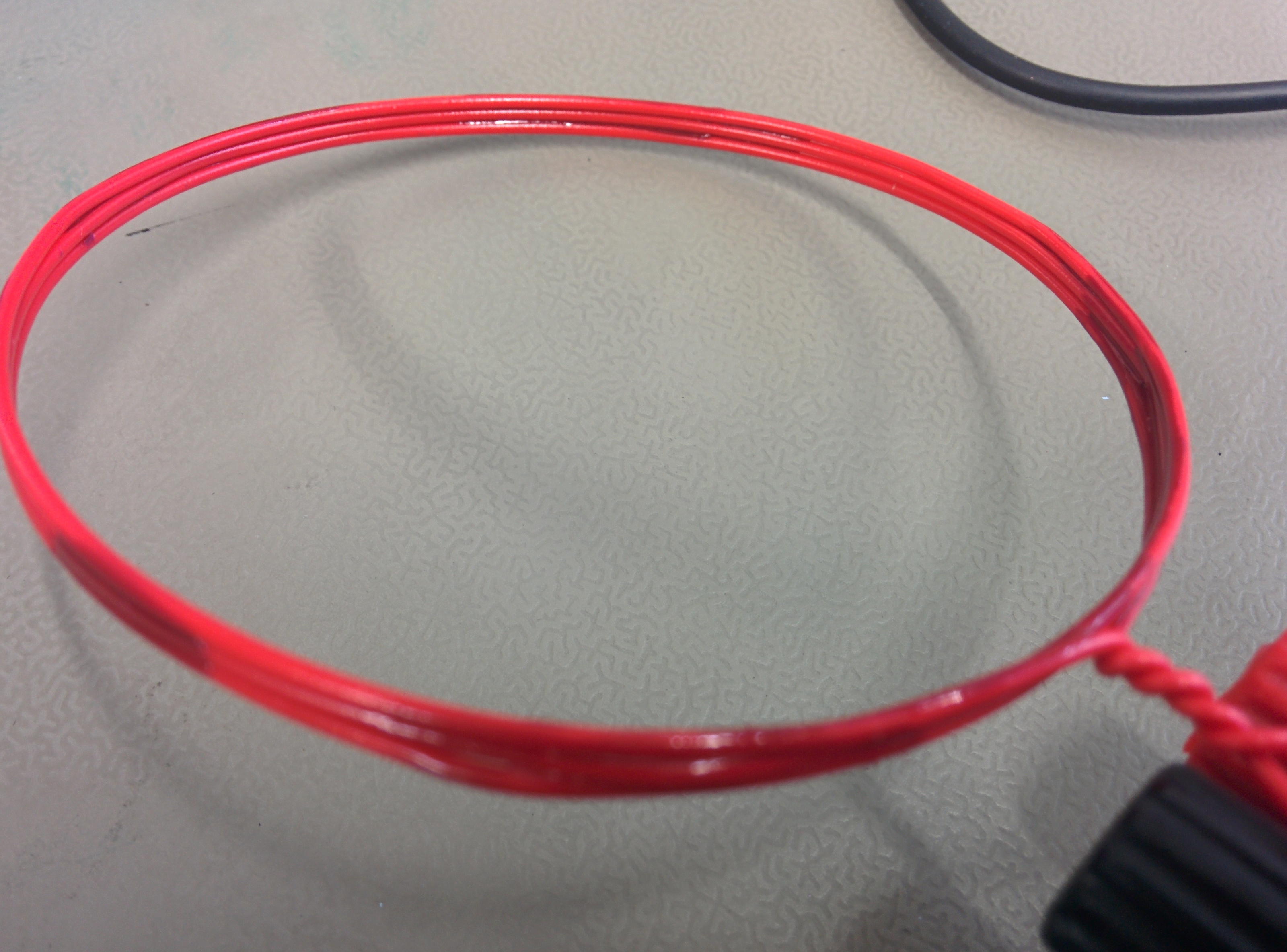
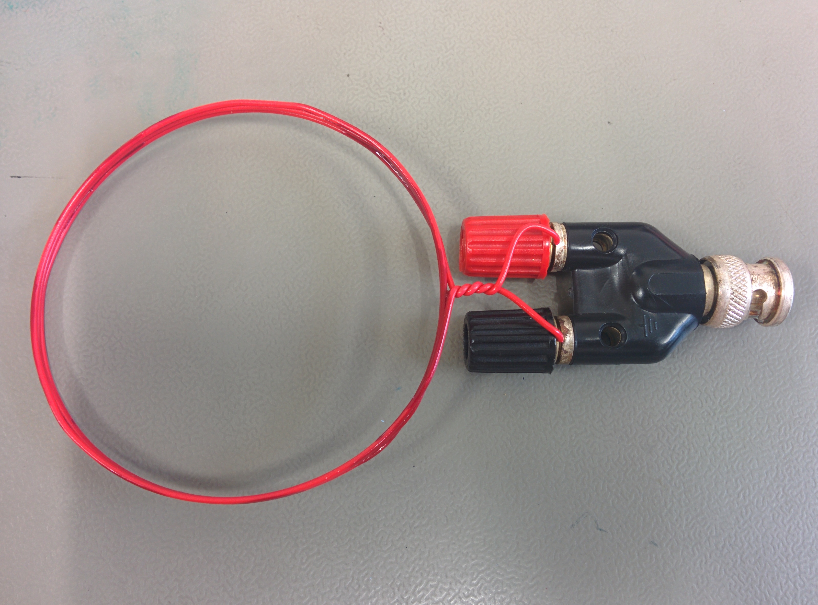
To monitor what the magnetic field was doing, I took a piece of wire, wound it around a small plastic bottle, and used some coil-dope to hold it all in place. The coil was not resonant, which probably deteriorates performance somewhat, and was arbitrarily chosen to have 3 turns. The diameter is approximately 80 mm.
 |
 |
Clicking on any of the pictures will load the picture details page. Click on the picture there, and it will show full resolution.
I then fed the coil output, via a BNC terminated coaxial cable, into a Tektronics MDO4104-6 scope. I have saved a few screenshots which show the sorts of output expected.
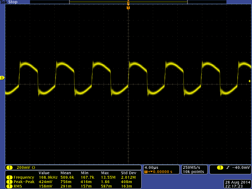
With an input impedance of 1MΩ, the coil output shows lots of ringing, probably due to the unmatched impedances of the loop, coax and scope input.
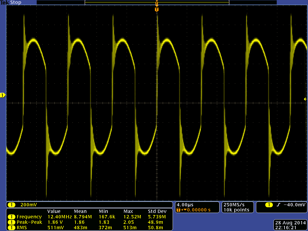
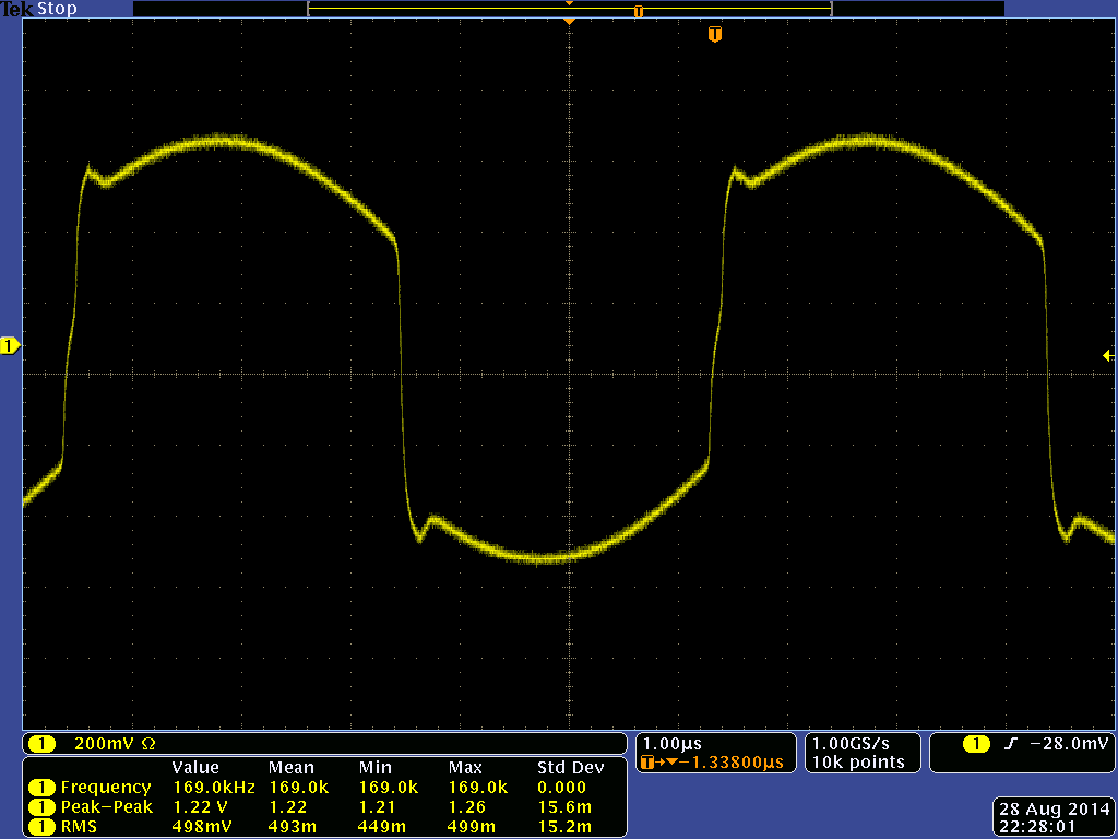
This ringing is easily rectified by switching the scope to an input impedance of 50Ω, although this clearly loads the loop.
We can see from the figure above that the frequency is 168.9 kHz, although the frequency doesn’t appear to be overly stable (range of around 154-223 kHz). We see a voltage mean of 1.12 V pk-pk into 50Ω. The figure below shows a zoomed view of one and a half periods.
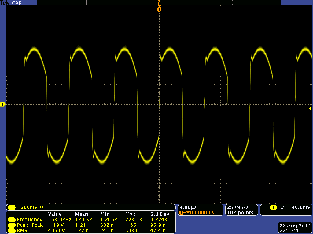
Keeping with the 50Ω input impedance, it is possible to see the phone is absorbing energy from the system. The peak-to-peak voltage is significantly reduced across the test coil.
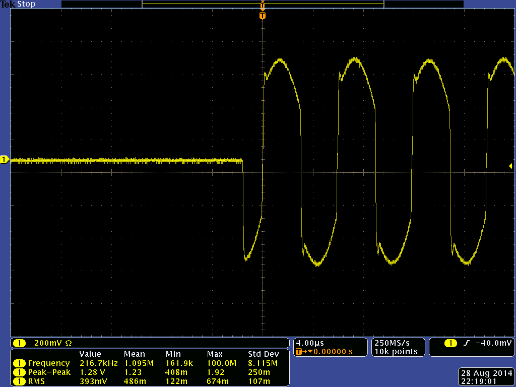
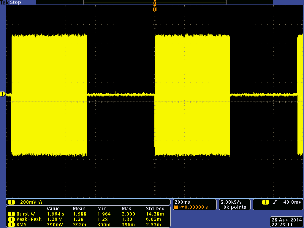
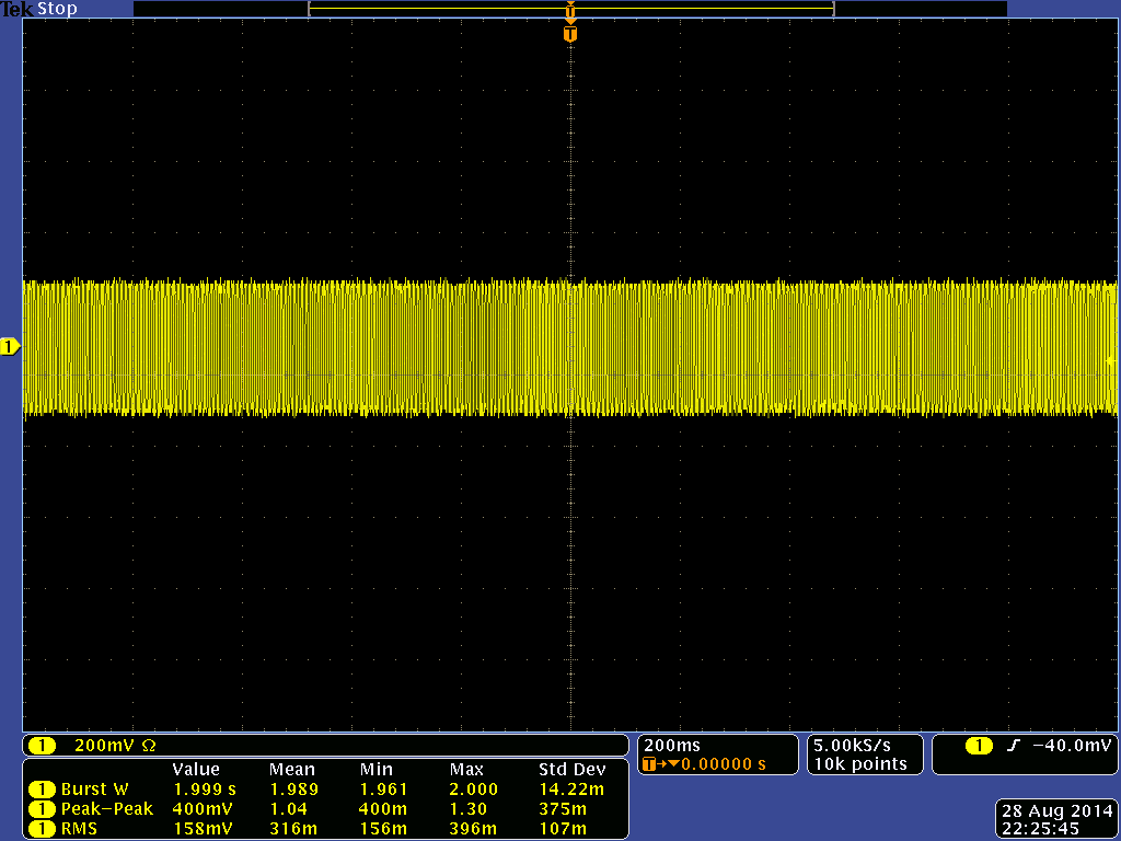
I noticed that with no phone present, the coil current was pulsed, meaning the waveform would be present for a time, and then absent for a time, with duty cycling taking place – probably to reduce the current drawn when no phone is connected. When the phone is presented, the waveform becomes continuous (at the reduced peak-to-peak level)
 |
 |
 |
Clicking on any of the pictures will load the picture details page. Click on the picture there, and it will show full resolution.